Binary logic devices
Binary Logic Notation
| Gate | Notation 1 | Notation 2 | Notation 3 | Notation 4 | Notation 5 |
|---|---|---|---|---|---|
| NOT | |||||
| AND | |||||
| OR | |||||
| NAND | |||||
| NOR | |||||
| XOR | |||||
| XNOR |
Logic Gates
| Logic Type | Logic Gate Symbol | Purpose | Design of Not Gate |
|---|---|---|---|
| NOT | 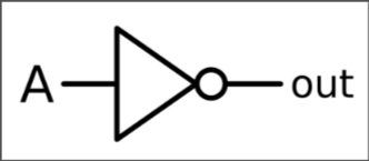 | Reverses the logic | 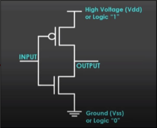 |
| AND | 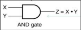 | Only if both input = 1, then output = 1 | 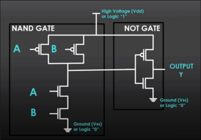 |
| OR | 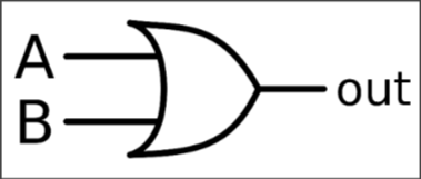 | If any input = 1, output = 1 | 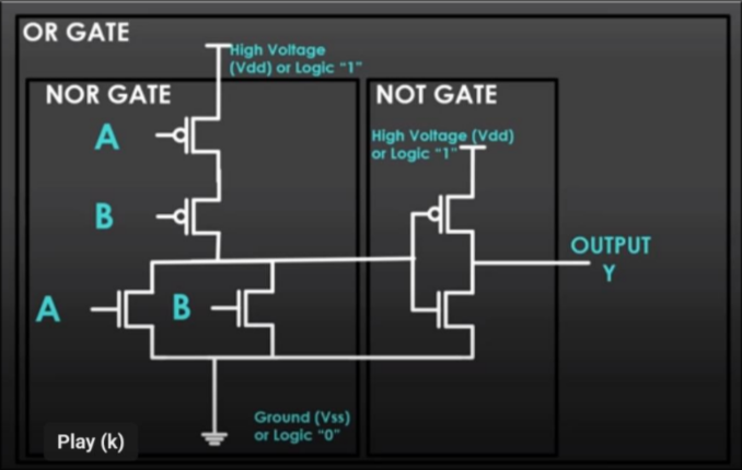 |
| XOR | 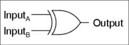 | If only 1 input = 1, output = 1 | 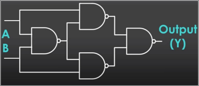 |
| XNOR | 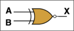 | inverse of XOR | 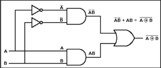 |
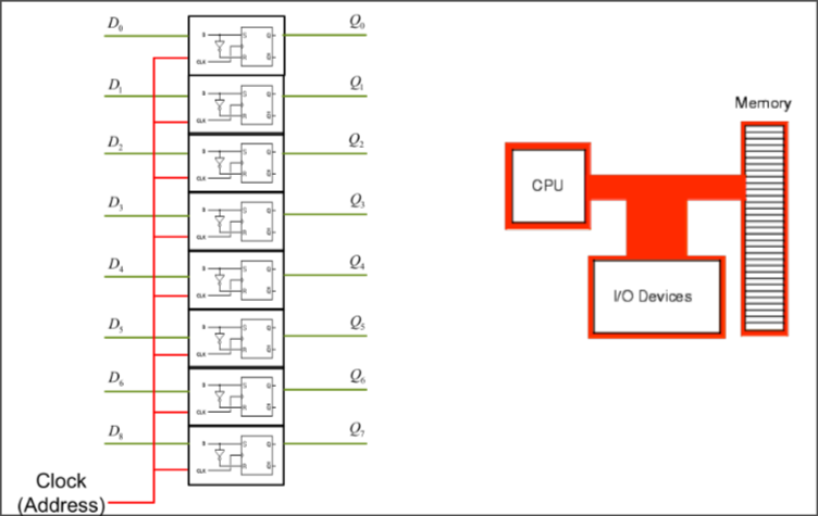
Registers
Single bit device
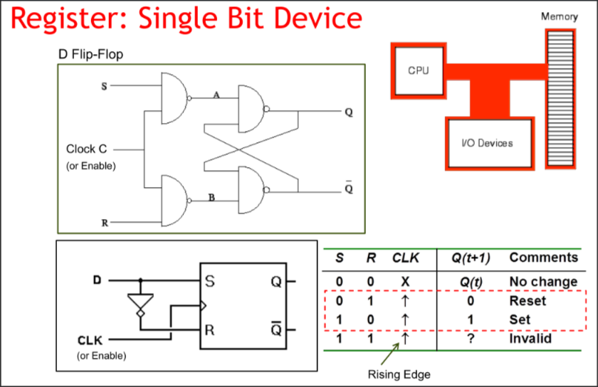
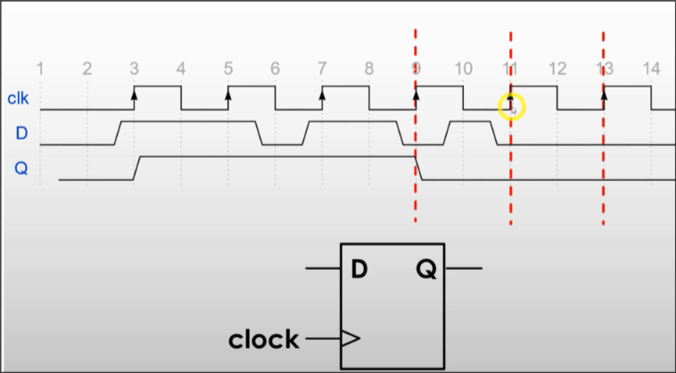
Clock Signals (enable)
Also know as the Rising Edge Trigger
- Only during an enable/rising-edge, will data be copied over from input to output
8-bit register
Basically 1-bit register x 8 to form a byte
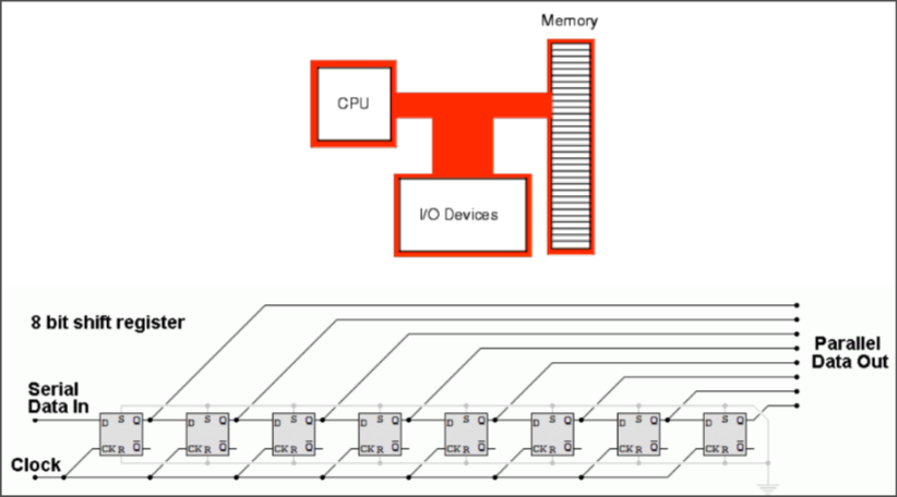
Shift register
When an input is received, the output is “shifted” to other registers to create a parallel output
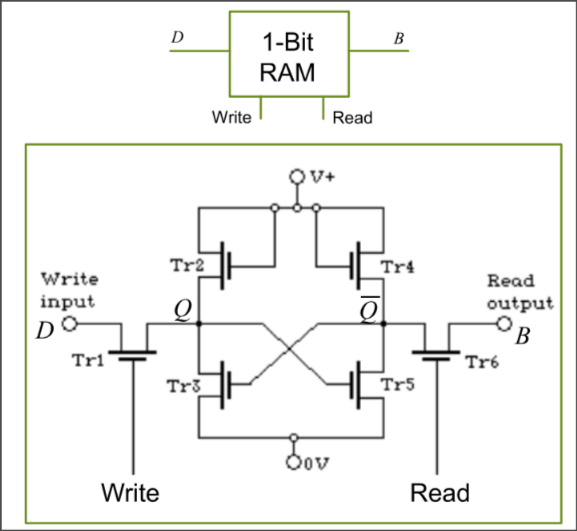
Memory Contruction
SRAM: Single bit static RAM
Storage is retained when power is cut
- e.g. solid state disk
- Drawback: cost
DRAM: Single bit dynamic RAM
Data is loss upon power loss
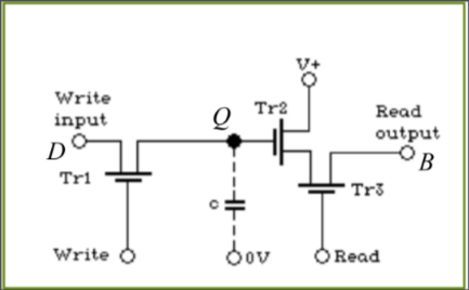
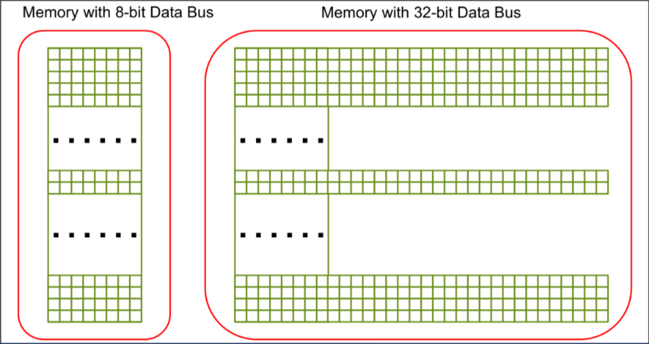
Data bus: each bit has its own data line
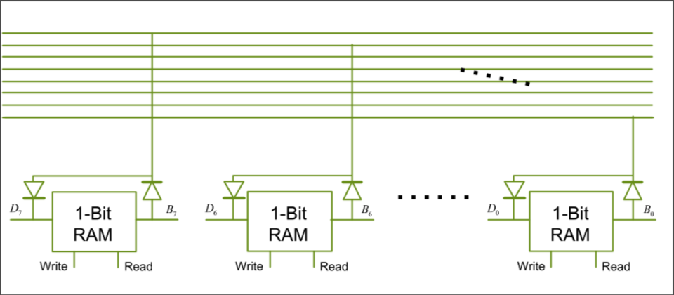
Flash Memory: 1 bit flash cell
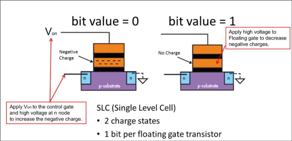
SLC(Single Level Cell): Has an extra floating gate
- 2 charge states
- 1 bit per floating gate transistor
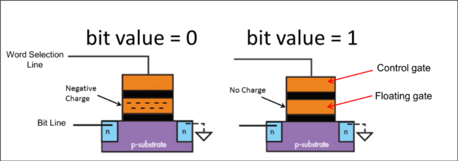
Inject electron to write 0 | “Suck out” electron to write 1
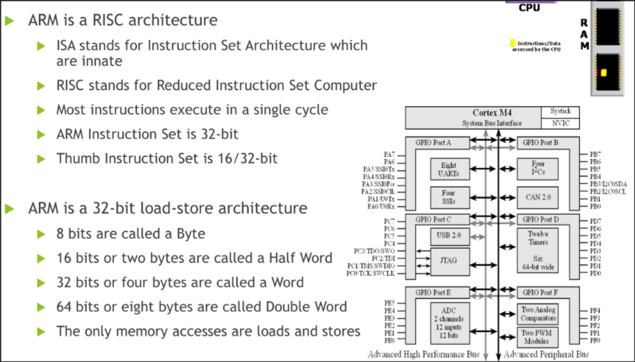
Memory unit
- Memory unit - set of bytes
- Byte - 8 bits
- Bit - one memory cell
Inputting data to memory unit
Inputting involves
- address of byte (Address Bus)
- data of one or more bytes (Data Bus)
The maximum amount of bytes a memory unit can have is determined by the number of values the address bus can output
- e.g. 64 bit address bus can have values
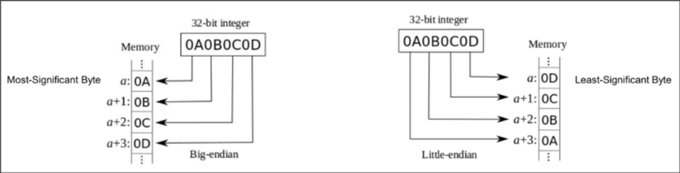
Endianness of Memory
Endianness is the ordering or sequencing of bytes of a word of digital data in computer memory storage or during transmission. Words may be represented in big-endian or little-endian manner. Big-endian systems store the most-significant byte of a word at the smallest memory address and the least significant byte at the largest. A little-endian system, in contrast, stores the least-significant byte at the smallest address.
- ARM with linux follows Little endian
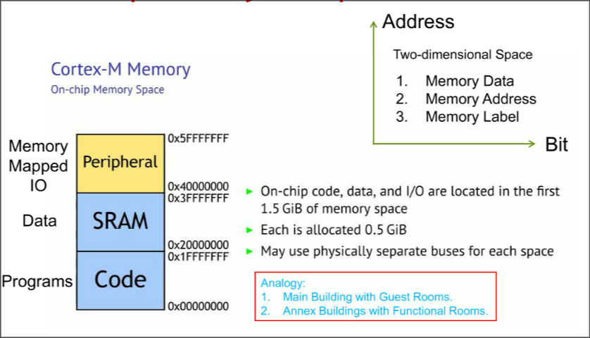
Memory Space in ARM
Recap
Registers of ARM
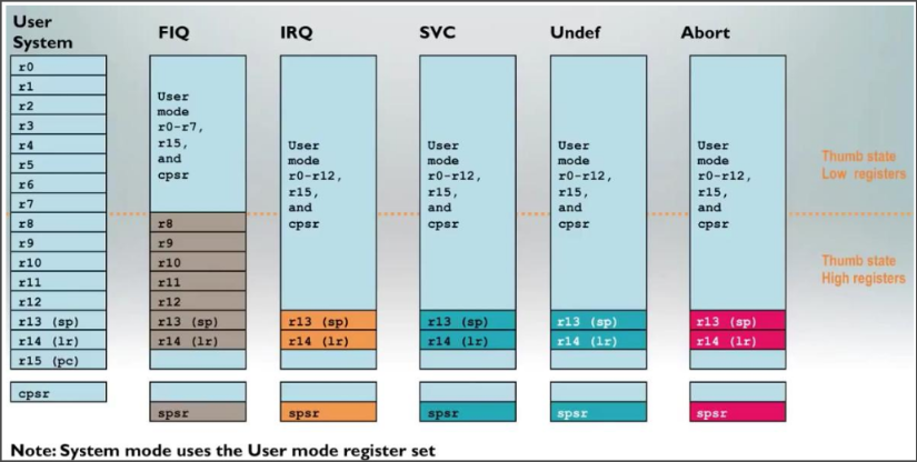
- PC: Program Counter
- LP: Link register (saved value of PC)
- SP: Stack pointer
- CPSR: Current Program Status Register
- SPSR: Saved Program Status Register
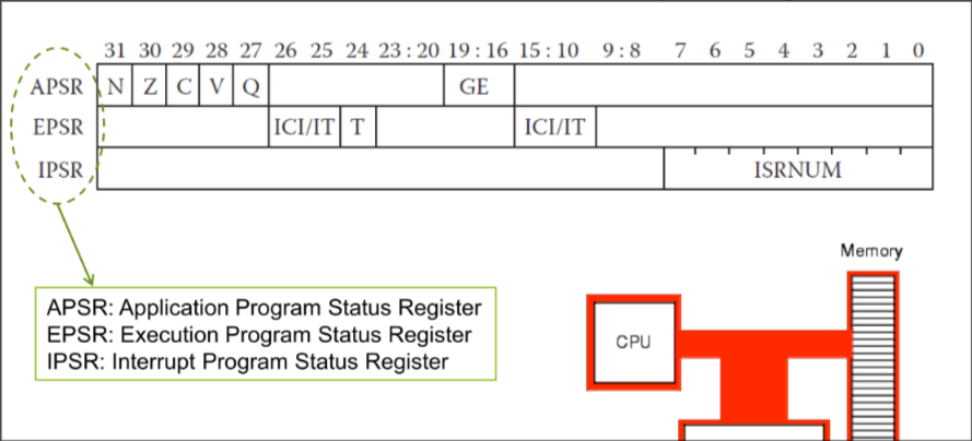
Program Status Register: R16
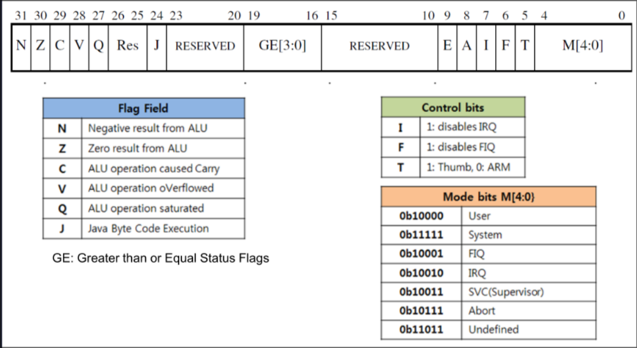
Cortex M4 Status Register
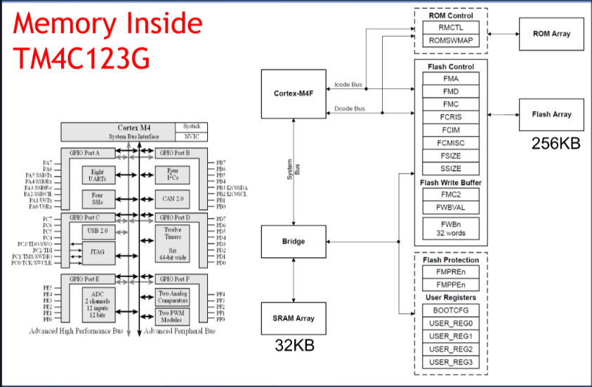
Memory inside TM4C123G
ARM Cortex-M Memory Space
On-chip Memory Sub-space in ARM
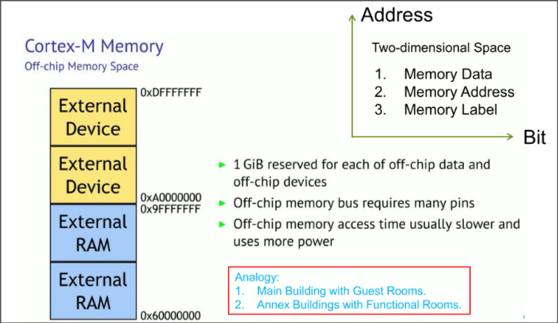
Off-chip Memory Subspace in ARM
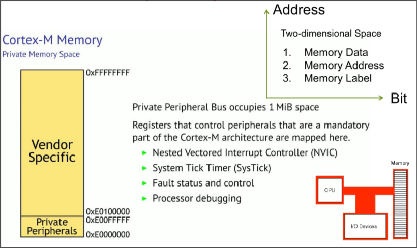
Private Memory Sub-space in ARM
Memory-Centric Operations
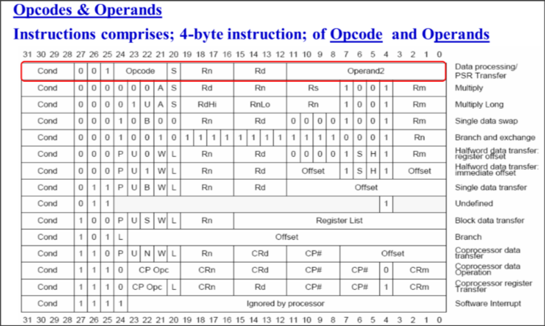
ARM’s instruction format
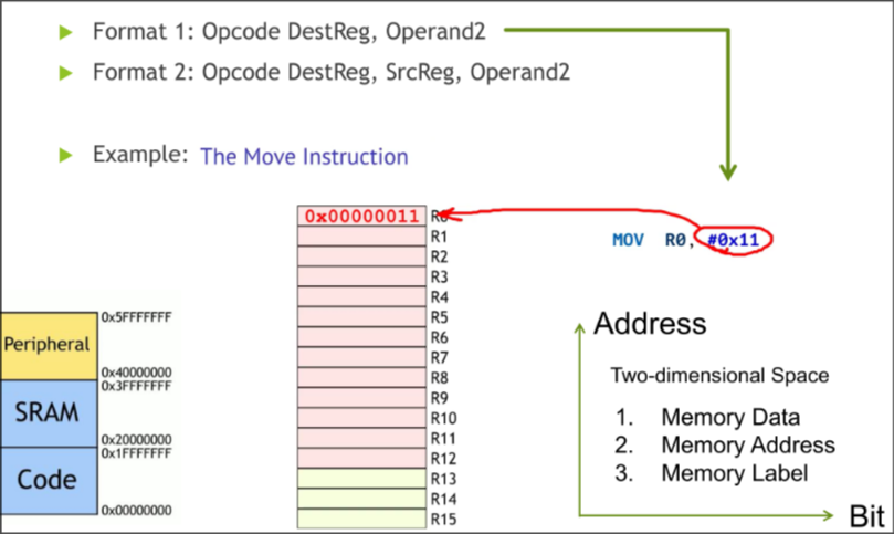
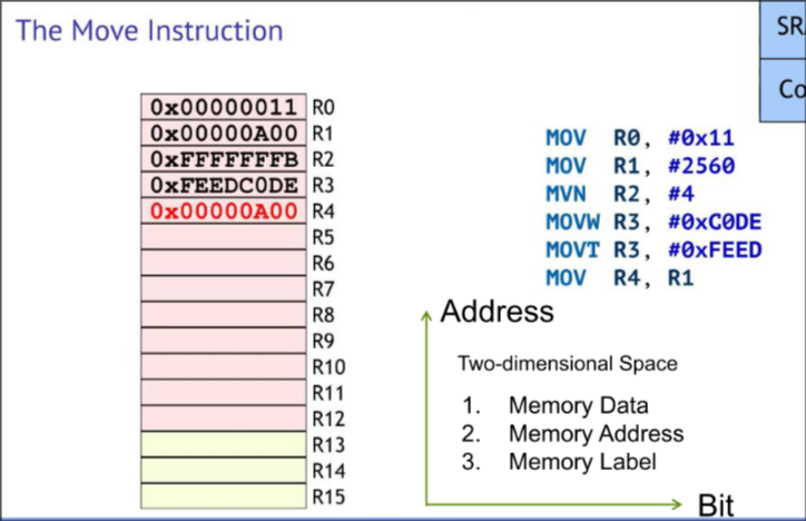
Moving data in ARM
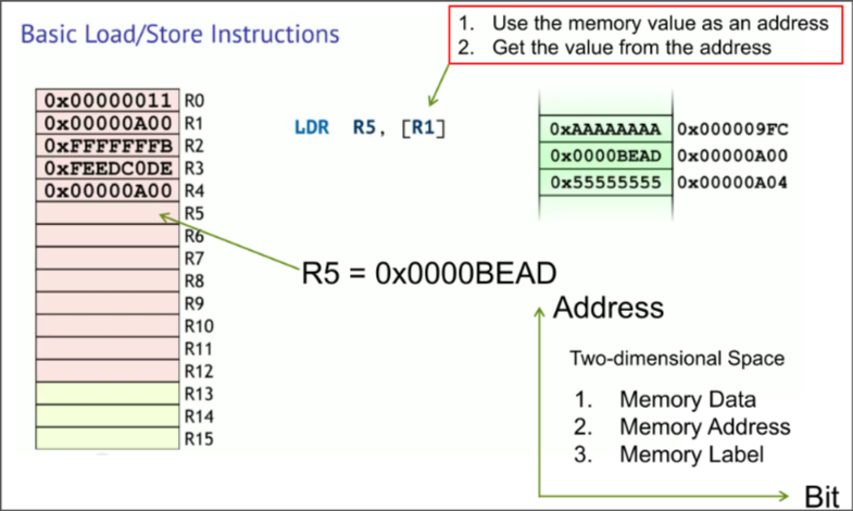
Loading operation in ARM
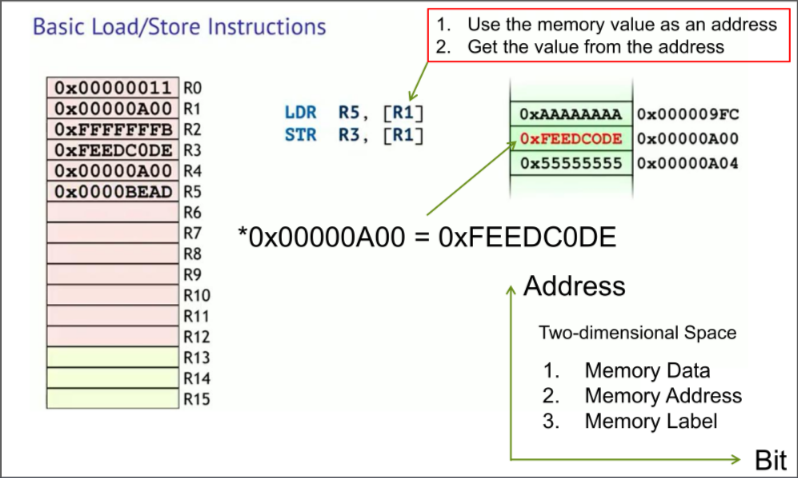
Store operation in ARM
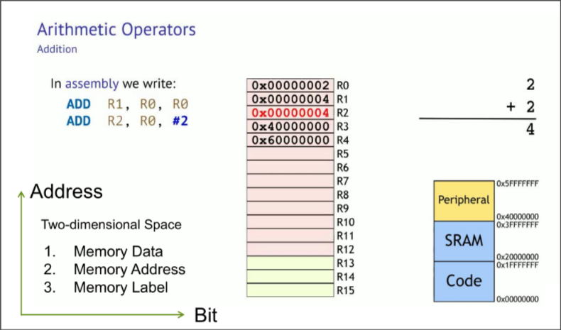
Addition in ARM
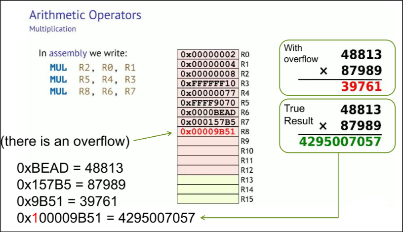
Multiplication in ARM
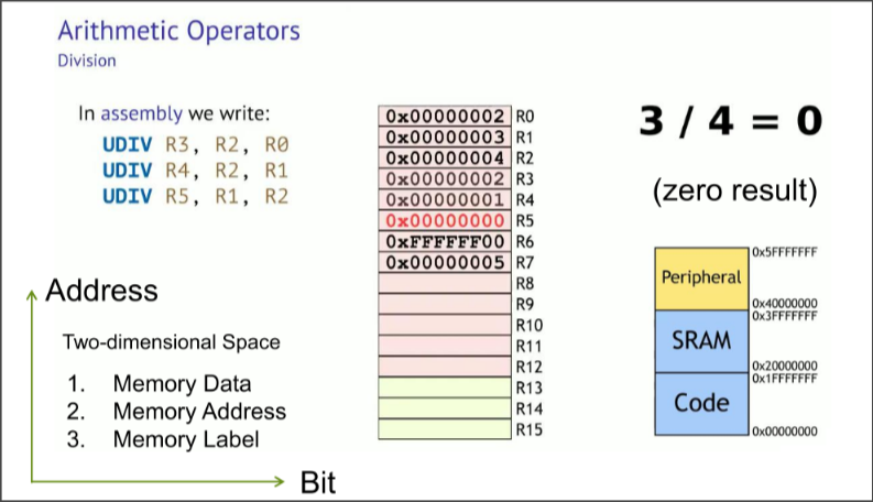
Division in ARM
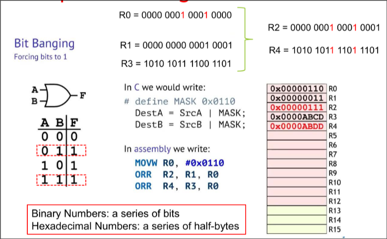
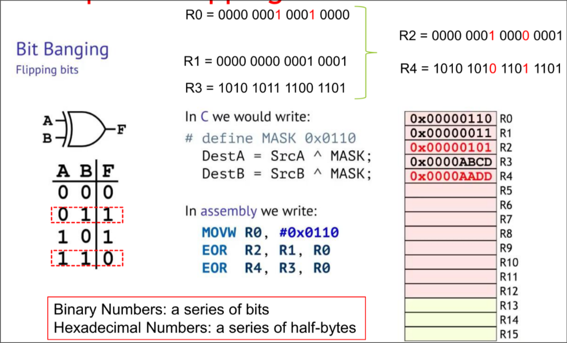
Forcing Bits to 1 in ARM
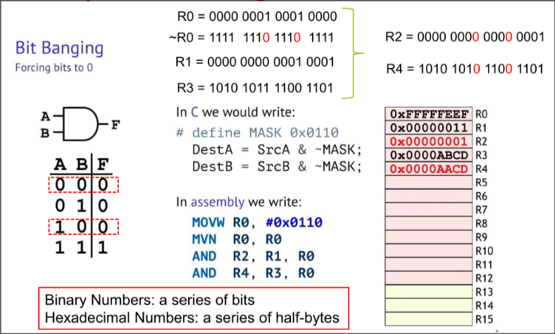
Forcing Bits to 0 in ARM
Flipping Bits in ARM
Memory-Mapped I/O Devices
Each I/O module has a port, which are all connected by Data Buses
In reference to ARM Cortex
Has two internal buses
The ARM Advanced Microcontroller Bus Architecture (AMBA) is an open-standard, on-chip interconnect specification for the connection and management of functional blocks in system-on-a-chip (SoC) designs. It facilitates development of multi-processor designs with large numbers of controllers and peripherals.
Supports Fast Interrupt Requests
An FIQ is just a higher priority interrupt request, that is prioritized by disabling IRQ and other FIQ handlers during request servicing. Therefore, no other interrupts can occur during the processing of the active FIQ interrupt
Supports Direct Memory Access
Direct memory access (DMA) is a feature of microprocessor systems that allows certain hardware subsystems to access main system memory such as RAM (Random Access Memory) independently of the central processing unit (CPU).
Includes a Debug Port
JTAG (Joint Test Action Group) specifies the use of a dedicated debug port implementing a serial communications interface for low-overhead access without requiring direct external access to the system address and data buses.
Cortex M4 Pin Diagram
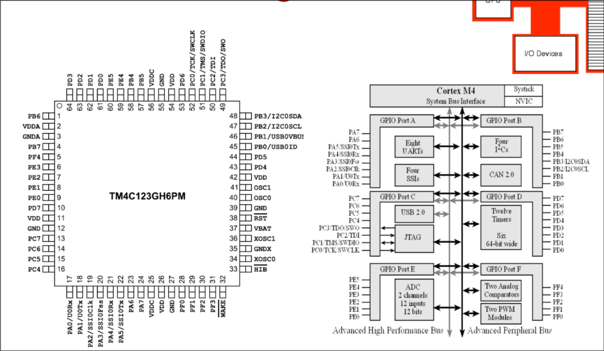
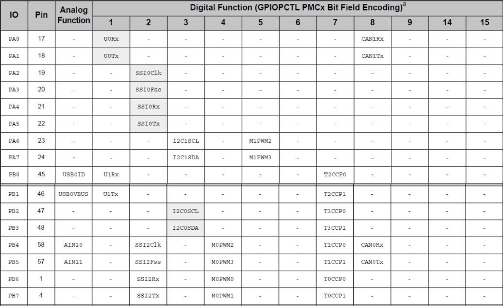
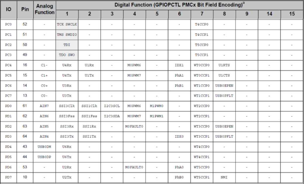
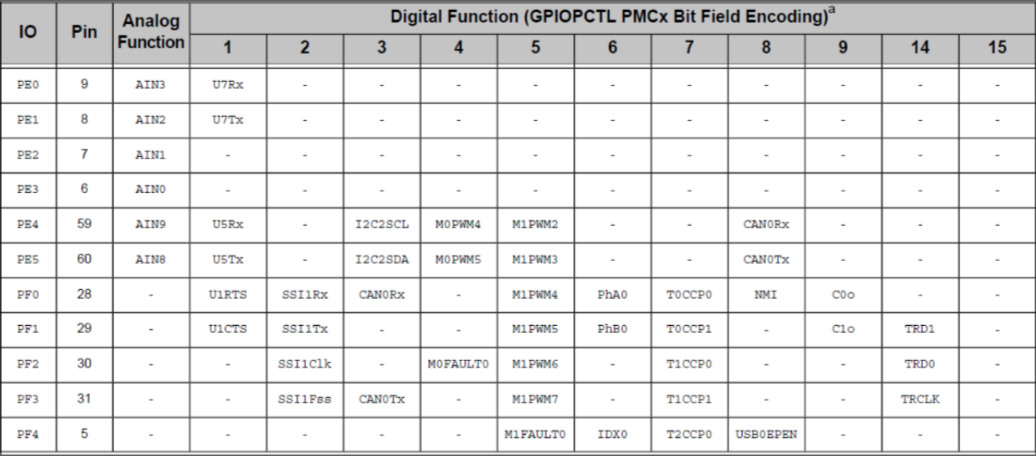
Blueprints
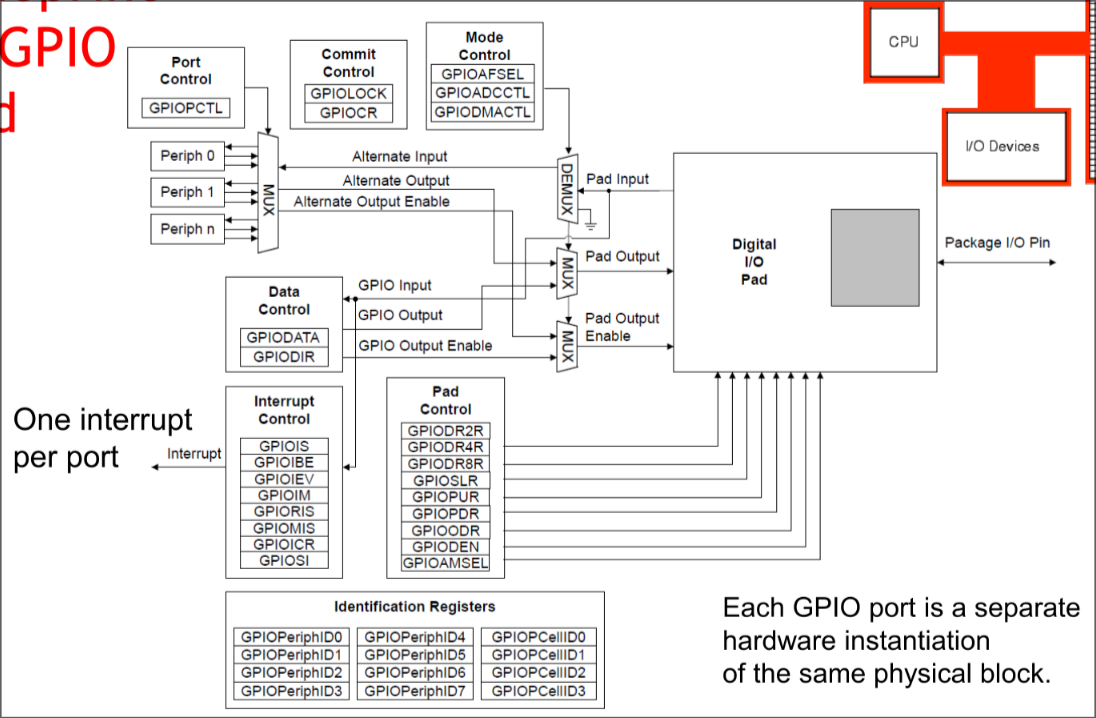
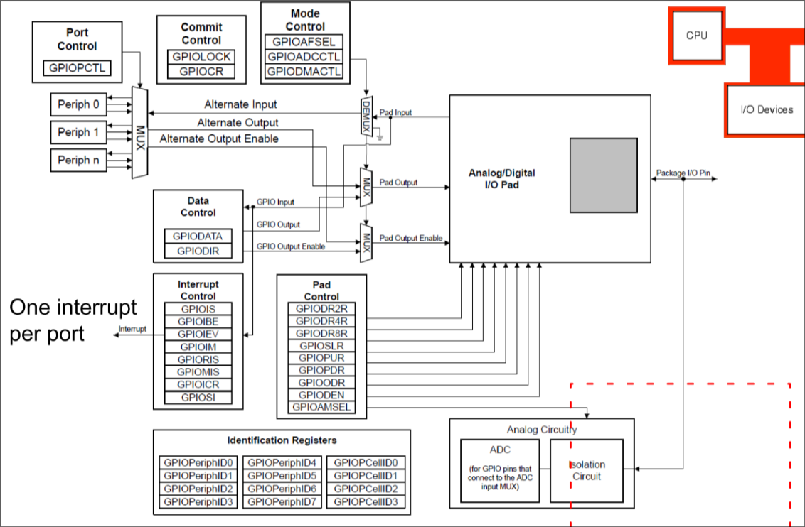
GPIO Pad
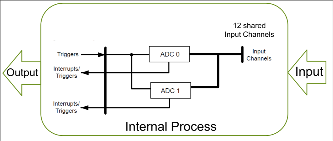
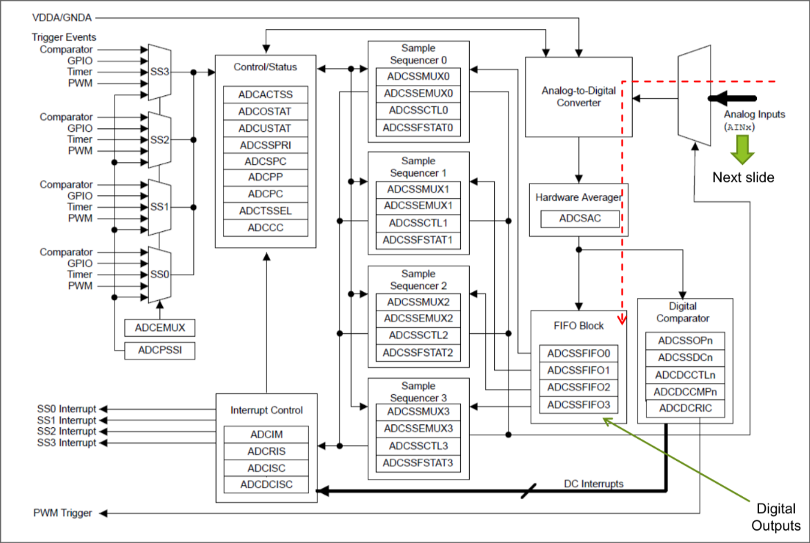
Analogue to Digital Conversion Block
ARM Cortex M4’s ADC
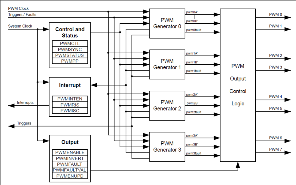
Cortex M4’s PWM Module
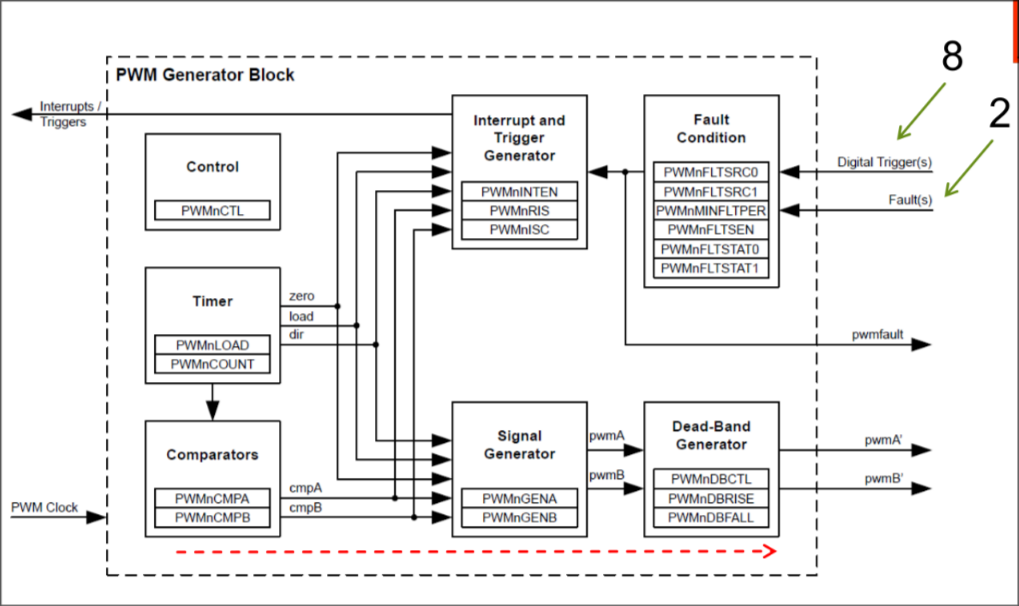
Of each PWM Generator
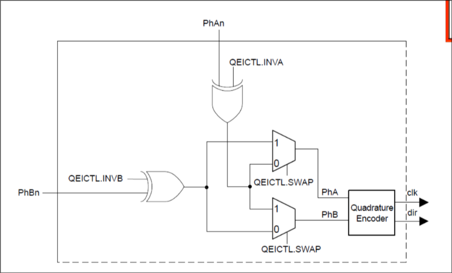
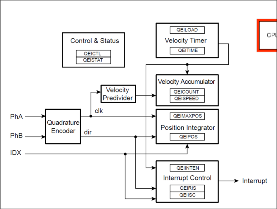
QEI Module
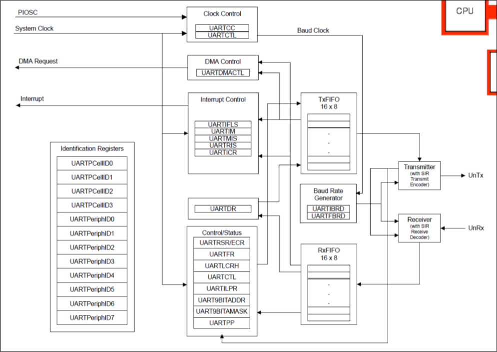
Cortex M4’s UART
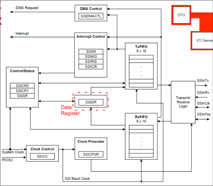
Cortex M4’s SSI
References
****