Structure of Crystalline Solids
Crystalline structures
-
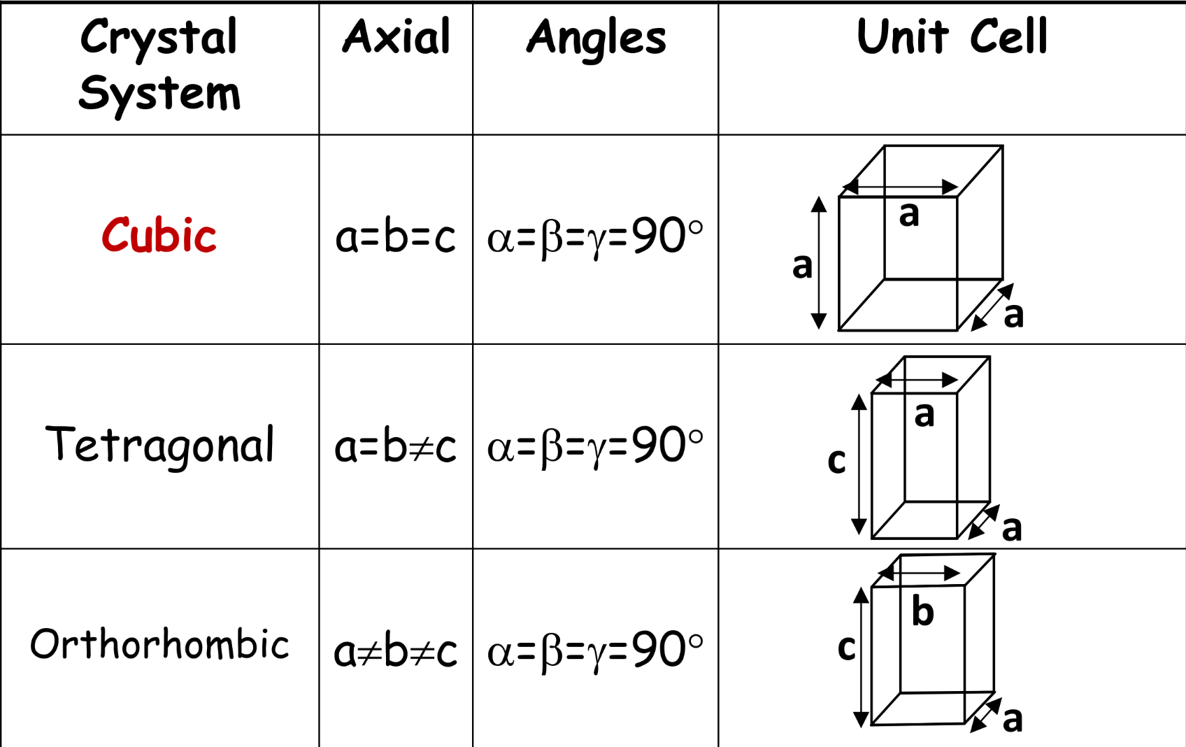
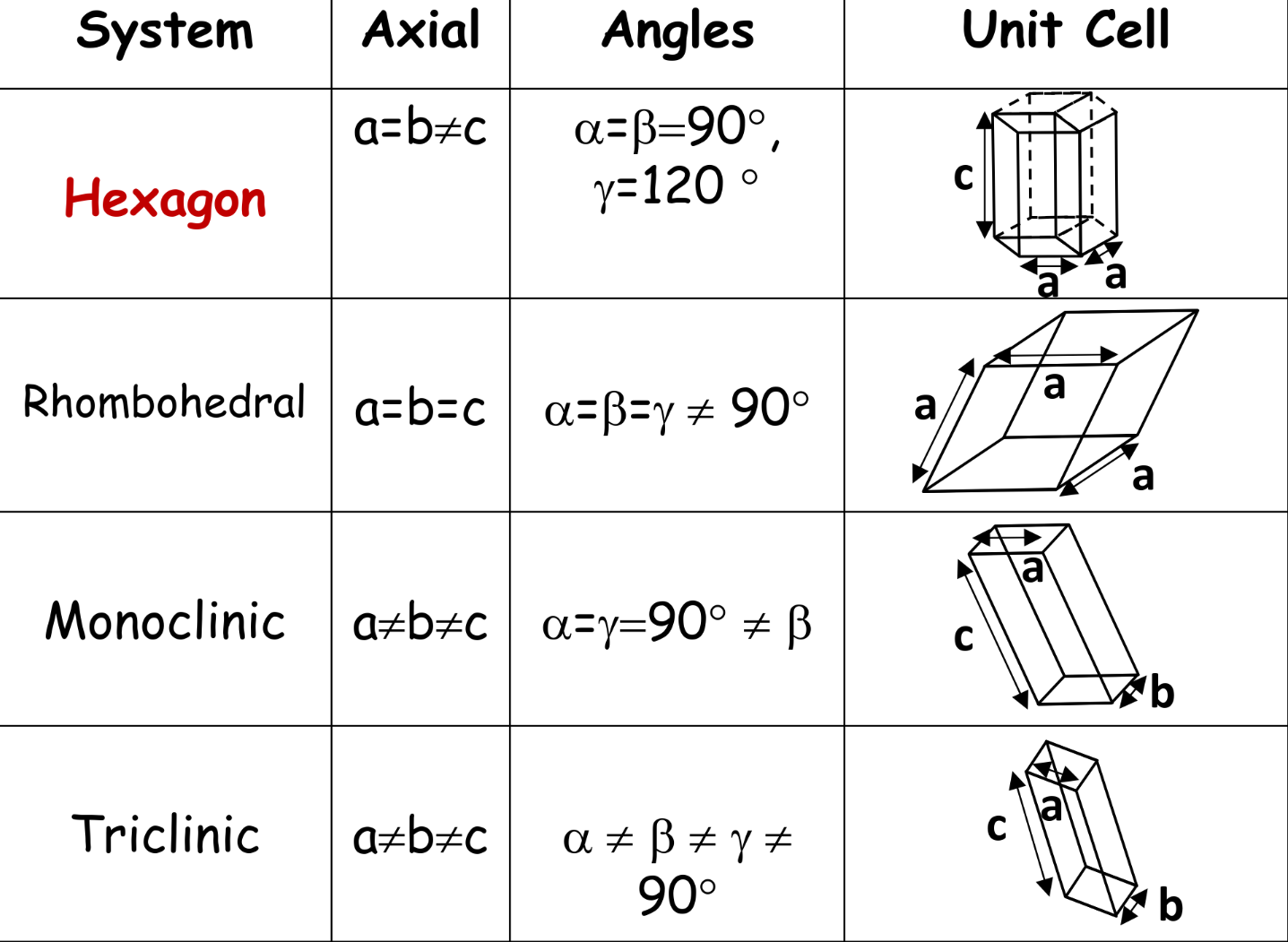
Seven crystal systems
-
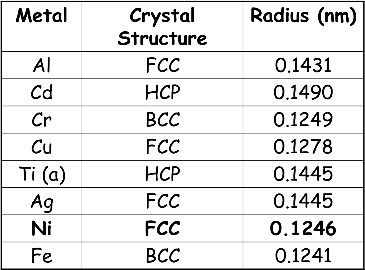
Common metal’s structure — Generally FCC, BCC and HCP
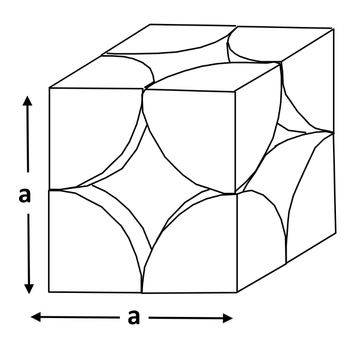
Simple Cubic
Cubic unit cell — atoms only at corners
-
1 atom per unit cell
Body-Centered Cubic (BCC)
Cubic unit cell — atoms at corners and single atom at center
-
Unit cell edge length (a) & atomic radius (R) is related
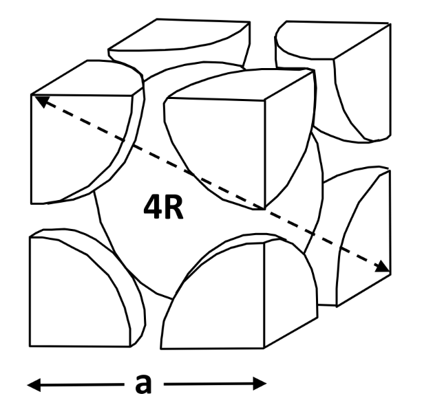
- 2 atom per unit cell — Coordination no. = 8 — APF = 0.68
APF (Atomic packing fraction) = density of atoms
CN (Coordination number) = number of neighbouring atoms touching an atom at a time
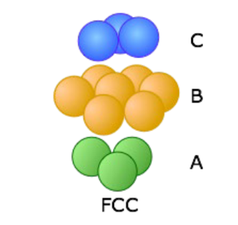
Face-Centered Cubic (FCC)
Cubic unit cell — atoms at corners and center of cube faces
-
Structure
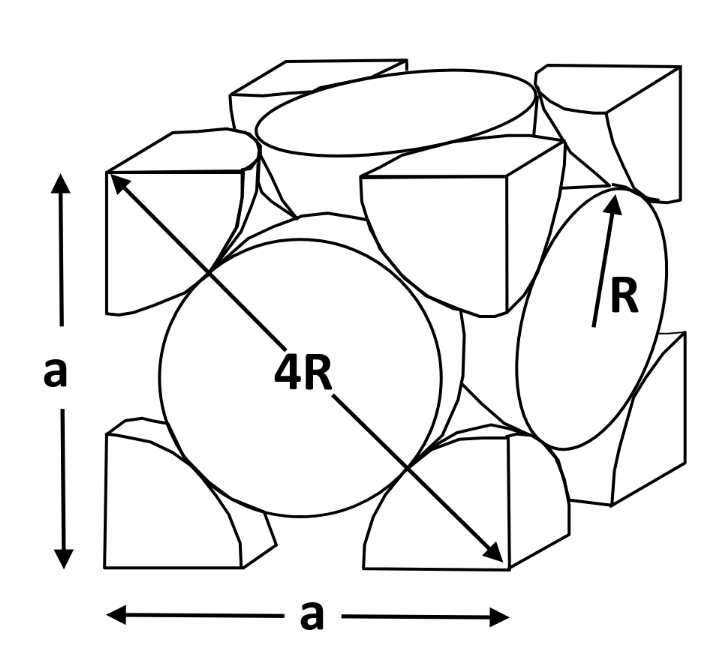
- 4 atom per cell — coordination no. = 12 — APF = 0.74
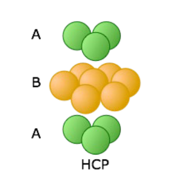
Hexagonal Closed Packing (HCP)
Hexagonal unit cell
-
Structure (c/a < 1.633)
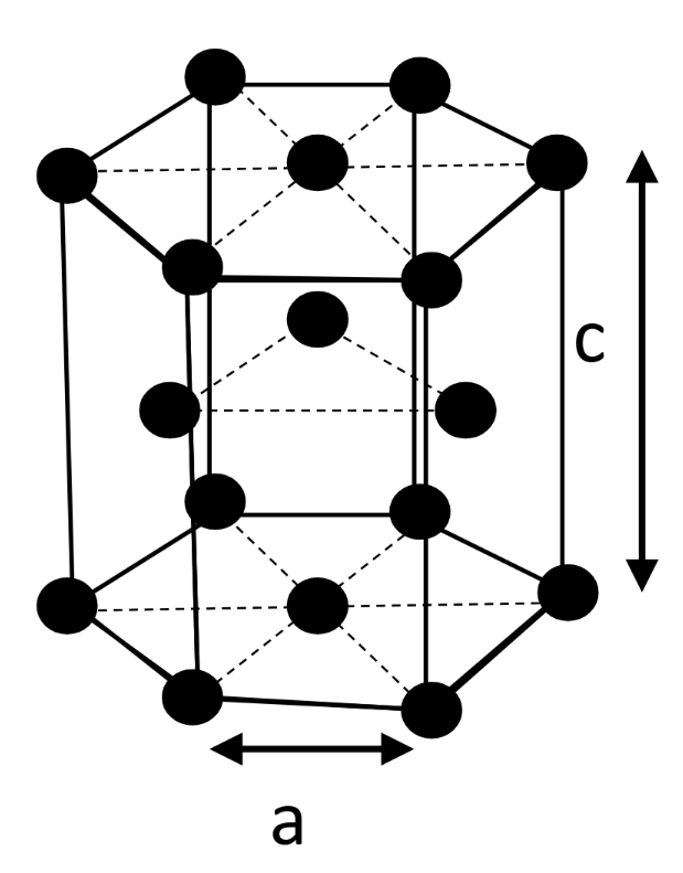
-
Coordination number 12 — APF = 0.74
Stacking & Packing Structures
-
ABA stacking
-
ABC stacking
Density of Unit Cell (p)
n = atom per unit cell = Avogadro’s number (6.023 x 10^23)
= Atomic mass = Volume of unit cell
Crystallographic Parameters
Crystallographic Direction
Important
- Bar above number indicates negative value
- Scale value to ≤ 1 for sketching Families of directions : vectors with the same magnitude
- symbolised by
- parallel directions are not unique
Crystallographic Planes
Set of parallel and equally spaced planes that pass through the centers of atoms in crystals where no centers are situated between planes
Miller indices: Symbolic vector representation for the orientation of an atomic direction or plane in a crystal lattice
- Described as (h k l) where “h,k & l” are miller indices
- Metal deformation are dependent on sliding of these planes — transportation of heat and electrons are also affected by them Miller indices for given plane
- Plane cannot touch origin / new origin — based on closest corner
- Find intercepts — reciprocal for plane miller indices
- E.g. intercept = -1 , -1/2, 1 → Draw plane given miller indices
- Reciprocal to find intercepts Family of planes
Crystallographically equivalent — Same packing density, atomic environment, physical & mechanical properties
- Indicated by {h k l}
- For cubic systems only, same indices = family
- (100) (010) (,0,0) — same family {100}
Linear Density
End point of vector does not cut the center
Planar Density
- Only area of atom within the plane is considered
Properties of Crystalline Solids
Defects in Solids
Point defects
Vacancies: site where atom is missing in lattice Self-interstitial: ‘extra’ atom between lattice site
The crystal structure aims to minimise strain, and thus the energy of the system (Gibbs free energy G), dependent on:
- Enthalpy (H): energy cost to break atomic bonds forming defect
- Entropy (TS): energy associated with no. of possible states Equilibrium concentration of vacancies @ T = constant (≠0) ARRHENIUS LAW n = number of defects — N = Number of atomic sites = activation energy of vacancy formation [J/mol.] or [eV/atom] k = Boltzmann’s constant, 1.38 x 10^-23 [J/atom/K] or 8.62 x 10^-5 [eV/atom/K]
Impurity(Alloy) — Interstitial & Substitutional Interstitial site positions in FCC:
- Octahedral — 1/2 1/2 1/2 — 0 1/2 1
- Tetrahedral — 1/4 3/4 1/4 Interstitial site positions in BCC:
- Octahedral — 1/2 1 0
- Tetrahedral — 1 1/2 1/4
Creation of point defects
- Annealing and abrupt quenching: “kinetically trapped point defects”
- Irradiation by high energy particles
- Ion implantation: useful for controlled doping of semiconductors
- Cold working
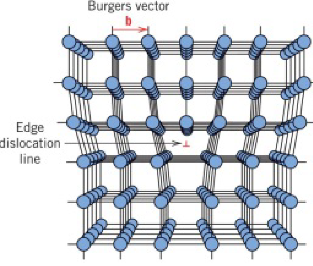
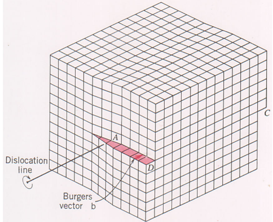
Line defects - dislocations
Burgers vector (b) — defines the magnitude and direction of lattice distortion of a dislocation
-
Edge dislocations
-
Screw dislocation
The two dislocations can mix
Interfacial defects - grain boundaries
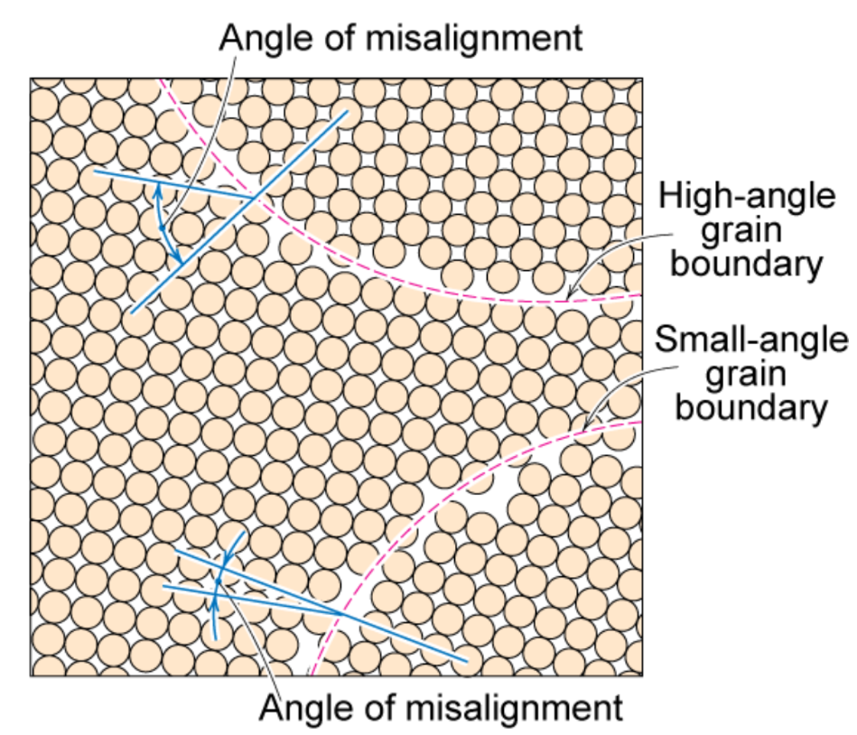 Grains can be — equiaxed (similar size) & columnar (elongated grains)
- Columnar in area with less undercooling
- Equiaxed in area with rapid cooling (near wall)
- Can be large like single crystal of diamond, or small enough to require microscope Optical Microscopy — Grains
- Polishing to remove surface features (scratches)
- Etching to change reflectance depending on crystal grain orientation
- Difference in reflectance differenciates individual grains Optical Microscopy — Grain boundaries
- The surface undergoes Acid Etching which attacks the grain boundaries
- This shows up as dark lines under the microscope
- Polarized light can increase this contrast Electron Microscopy
- Optical resolution = 100nm
- High frequency → Higher resolution
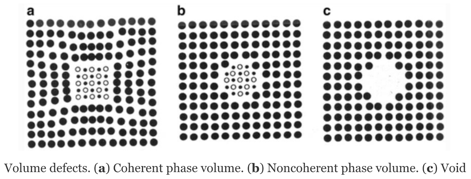
Bulk & Volume defects
Dislocations
Plastic deformation is due to movement of dislocations — slipping in the direction of burgers vector
- Dislocations increase G proportionally to b
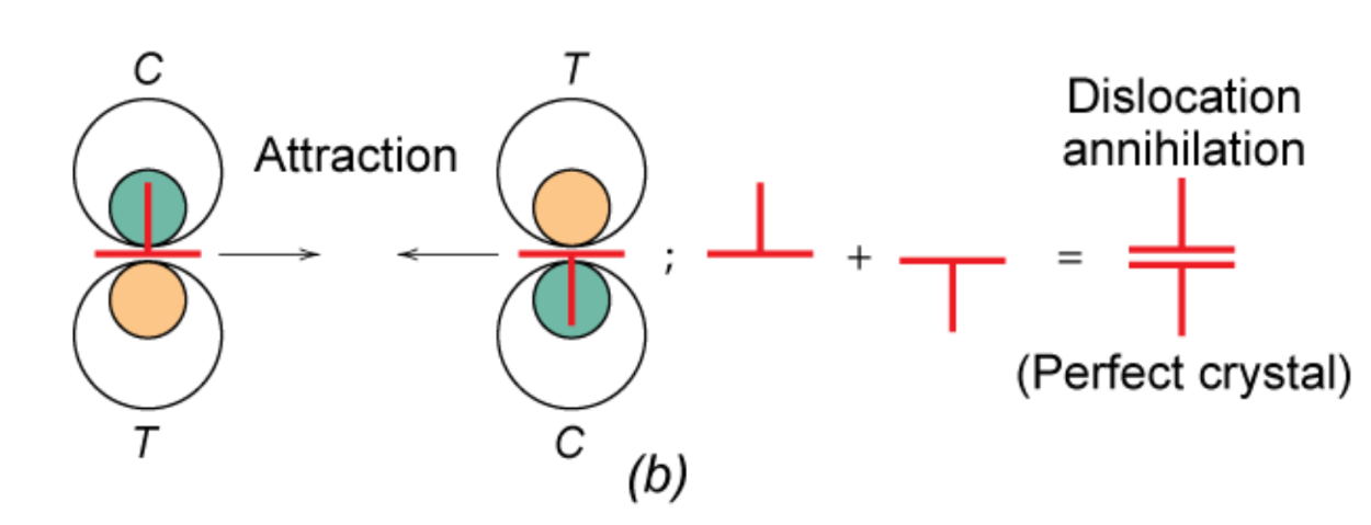
- Dislocations of the same sign repel while opposite signs attract and annihilate
- Energy required to move dislocation is related to burgers vector b
- Thus preferred direction is one with minimum b
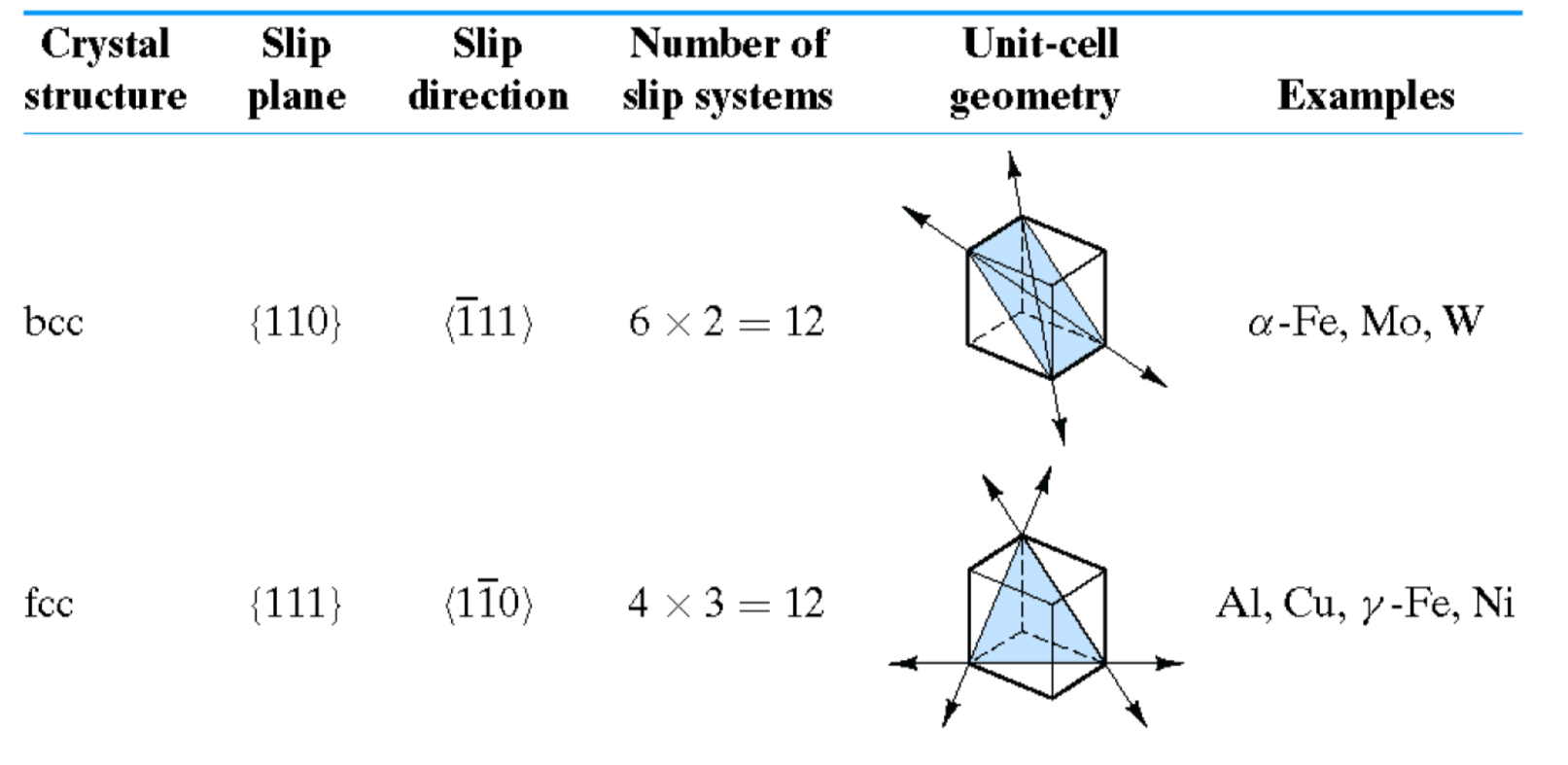
Slip systems
- Slip planes — easiest slippage due to high planar density
- Slip directions — along burgers vectors
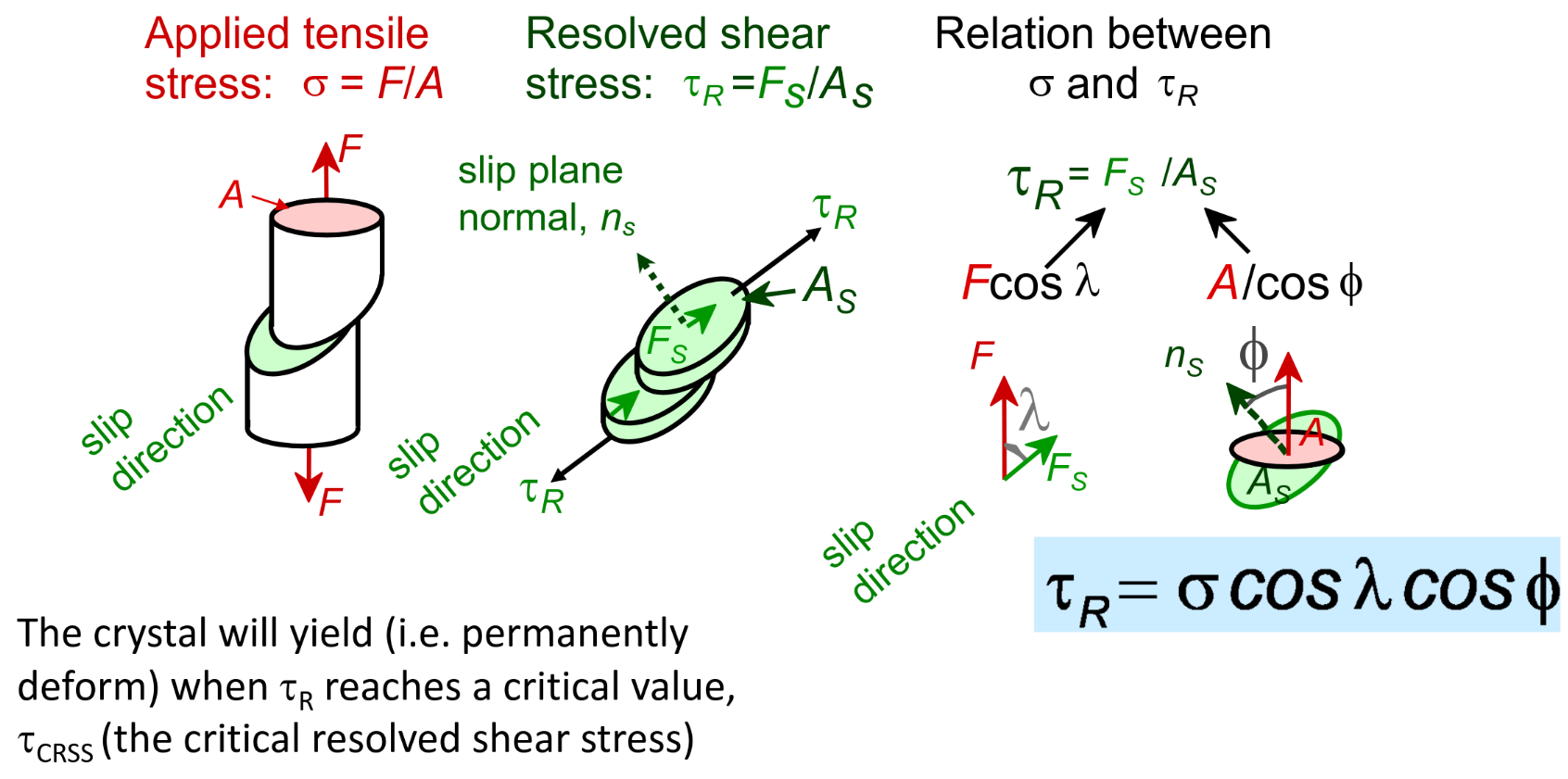
Resolved shear stress
Deformation of ceramics
-
Most fracture before plastic deformation
-
Brittle → ionic bonds → difficult to slip due to repulsive coulombic forces between + - ions
-
ionic and covalent materials are brittle and display no plastic deformation
Mechanical properties of material
Hooke’s Law: Stress() - strain(): Recap:
- Stress → force / area
- Strain → % elongation
Engineering stress
Tensile stress → Stretch or compression force / area of interest Shear stress → shearing force / parallel area of interest
- includes torsion
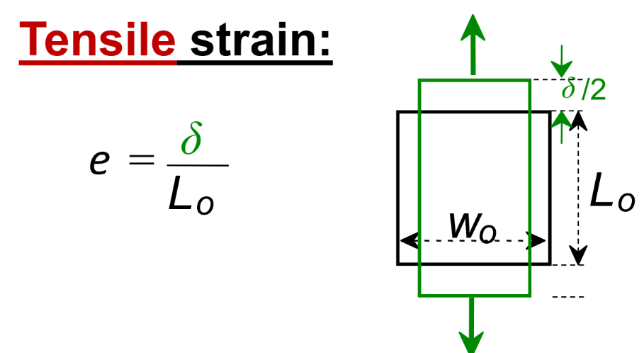
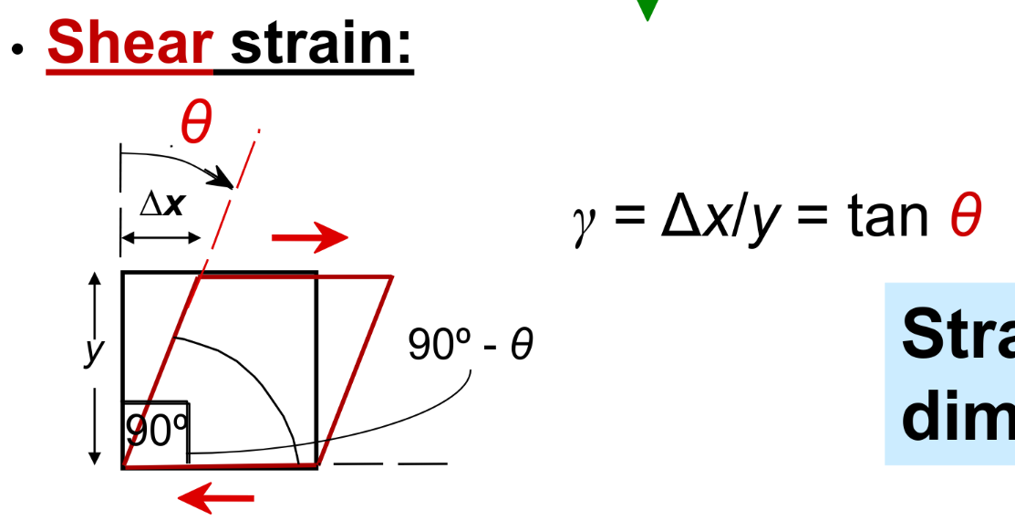
Engineering strain
 Poisson’s Ratio → a ratio describing the contraction perpendicular to extension due to tensile stress
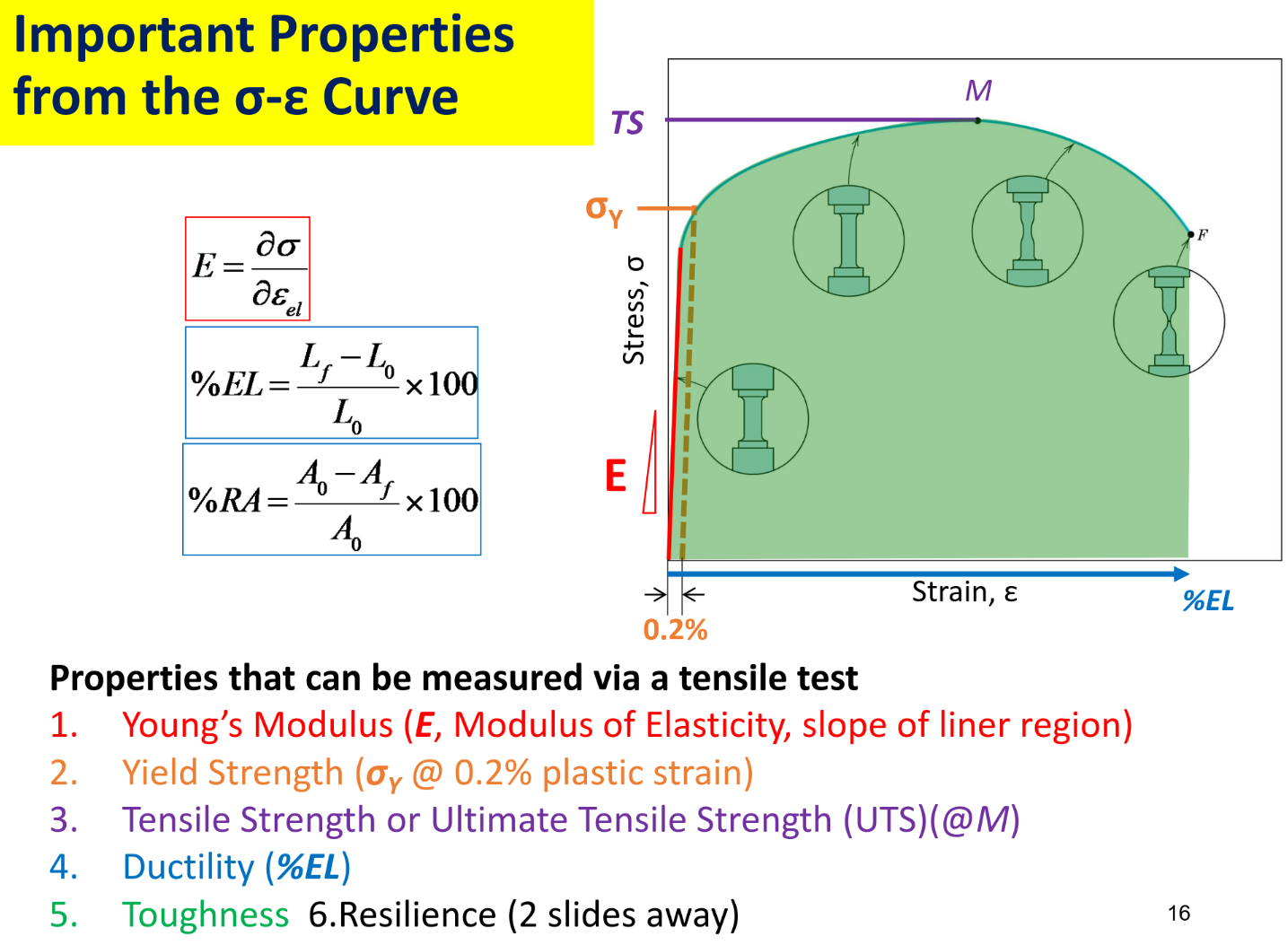
Stress-strain curve: tensile test
 Resilience / Elastic strain energy
For linear elastic:
Resilience / Elastic strain energy
For linear elastic:
-
AKA area below linear region with reference to yield strength Yield strength
-
stress at which noticeable plastic deformation occurs
- Happens due to slipping of planes
-
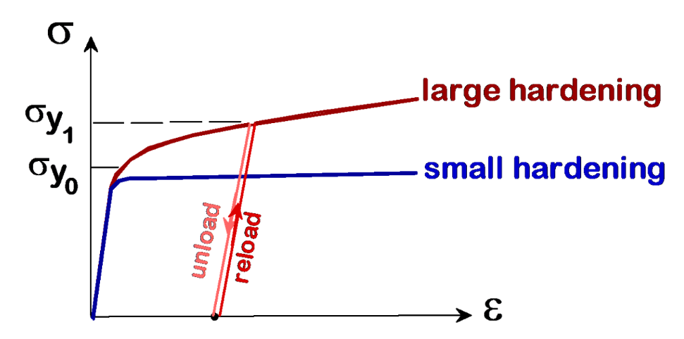
Can increase with Work Hardening / Strain Hardening
-
Due to plastic deformation
-
Toughness: energy required to break a unit volume of material
- Brittle(low toughness) → high yield strength but %EL — ceramics
- Tough → good yield strength and %EL — metals
- Ductile(moderate toughness) → large %EL but very low yield strength — soft polymers
- Brittle fracture — elastic energy dominant
- Ductile fracture — plastic energy dominant
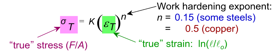
True stress and strain
In the engineering graph, it curves down as the cross-sectional area rapidly decreases within neck region at the strain limits, making the material appear to weaken when it is actually strengthening
True stress vs engineering stress: True strain vs engineering strain:
Hardness
Resistance against denting
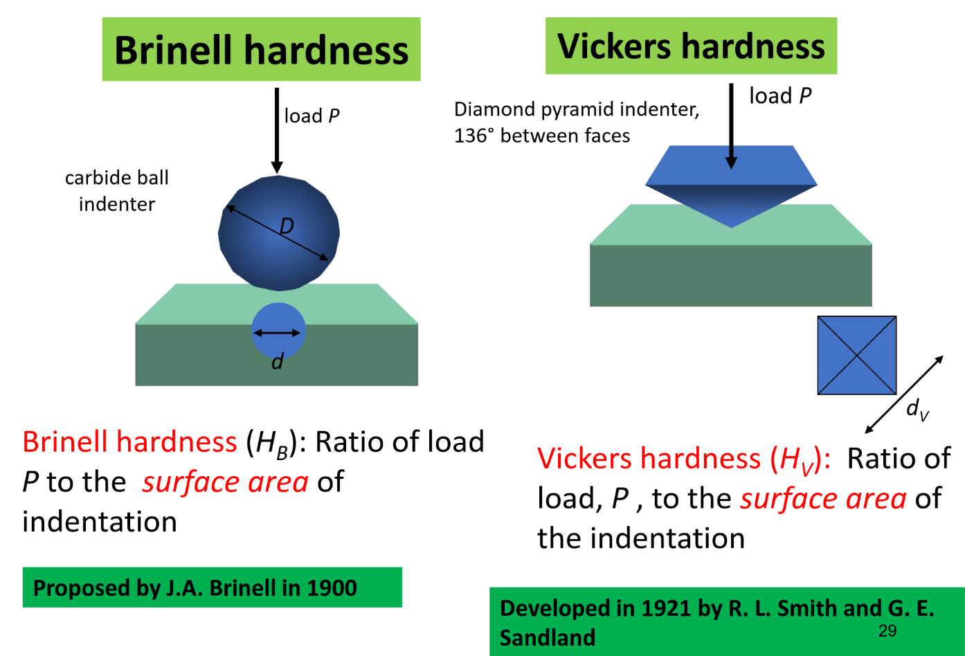 Advantages of hardness test:
- Simple & inexpensive — Non-destructive — can extrapolate other data from hardness
Strengthening Mechanisms
Design principle: Increase intrinsic resistance to dislocation motion to reduce plastic deformation
Grain boundary strengthening
At < 0.5 melting temperature, grain boundaries restrict dislocation motion as it requires more energy/stress to slip past them
Smaller grain size → more barriers → higher stress to move dislocations → higher strength Hall-petch Relation
Solid solution strengthening
Impurities distort lattice & generate lattice strain that act as barriers to dislocation motion
- Partially cancels out compressive/tensile strength of dislocations
Strain hardening (cold work)
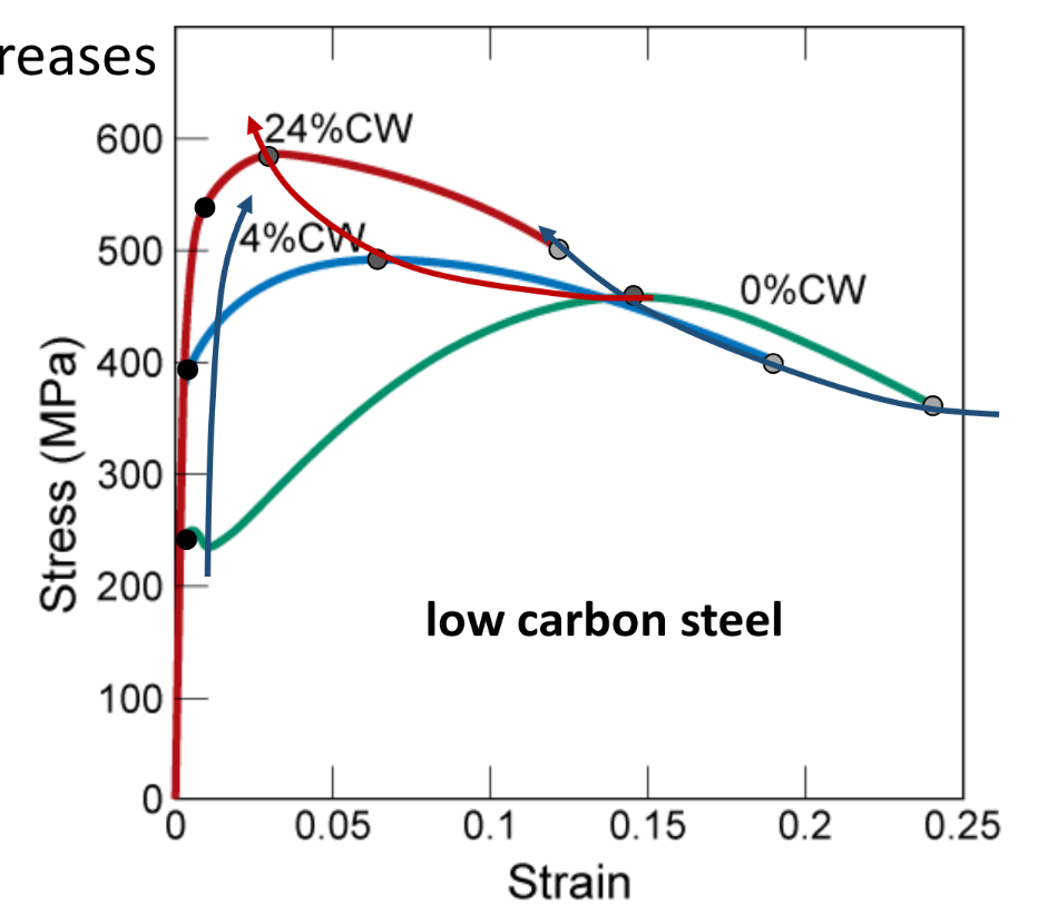 Yield strength increase
Tensile strength increase
Ductility decrease
Yield strength increase
Tensile strength increase
Ductility decrease
- Dislocations multiply significantly and entangle during cold work → reduced slipping
- Large deformation in cold working can make material too brittle
- Intermittent annealing (heating and holding at high temperatures) can restore ductility for further deformations
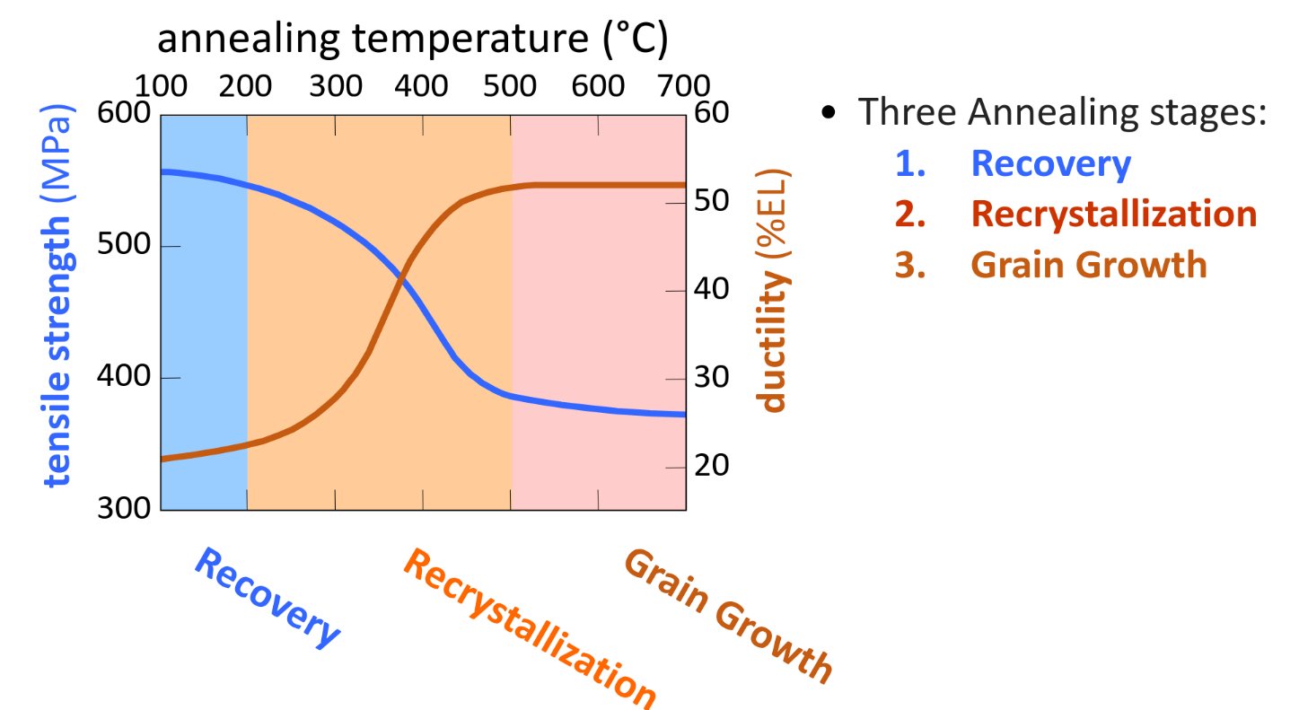 Recovery — reduction of dislocation density by annihilation
Results of higher temperatures:
Recovery — reduction of dislocation density by annihilation
Results of higher temperatures:
- Intermittent annealing (heating and holding at high temperatures) can restore ductility for further deformations
- easier atomic diffusion → atom can move to fill area of tension
- larger vacancy concentration → allow dislocations to climb into slip plane and annihilate Recrystallisation New grains formed with:
- low dislocation density — small in size — consume and replace parent cold worked grains
- Recrystallization temperature — Temp which it completes in 1h exactly
- Decreases with increasing %CW & increasing purity
- Hot working happens above this temp Grain growth — small grain shrink and assimilate with larger grains
Phase Diagram
When we combine two elements, with reference to the composition and temperature, what is the resulting equilibrium states and phases?
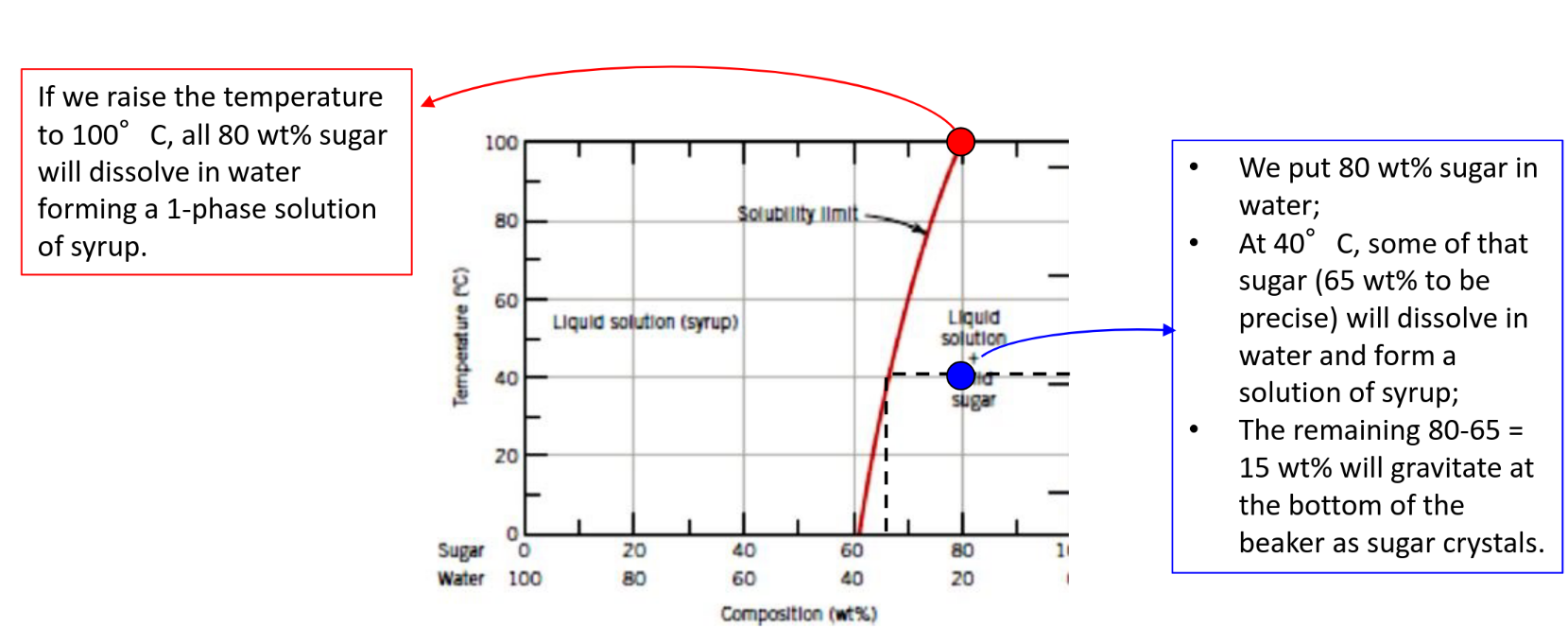
Solubility limit — Maximum concentration for which only a single phase solution exists
Solid Solution (Alloys)
Minority = Solute — Majority = Solvent
Equilibrium phase diagrams
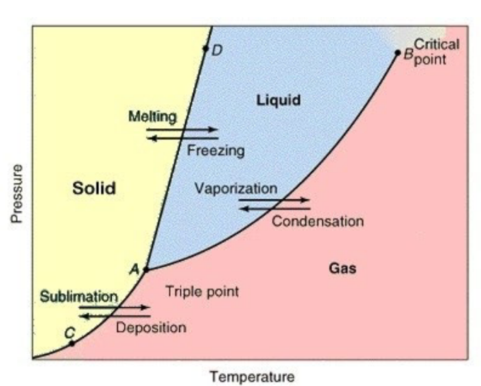
Unary Phase Diagram
Hume-Rothery rules - conditions to form complete solid solutions
- Atomic size factor — Difference in radii <
- Crystal structure — same type
- Electronegativity — similar
- Valency — similar
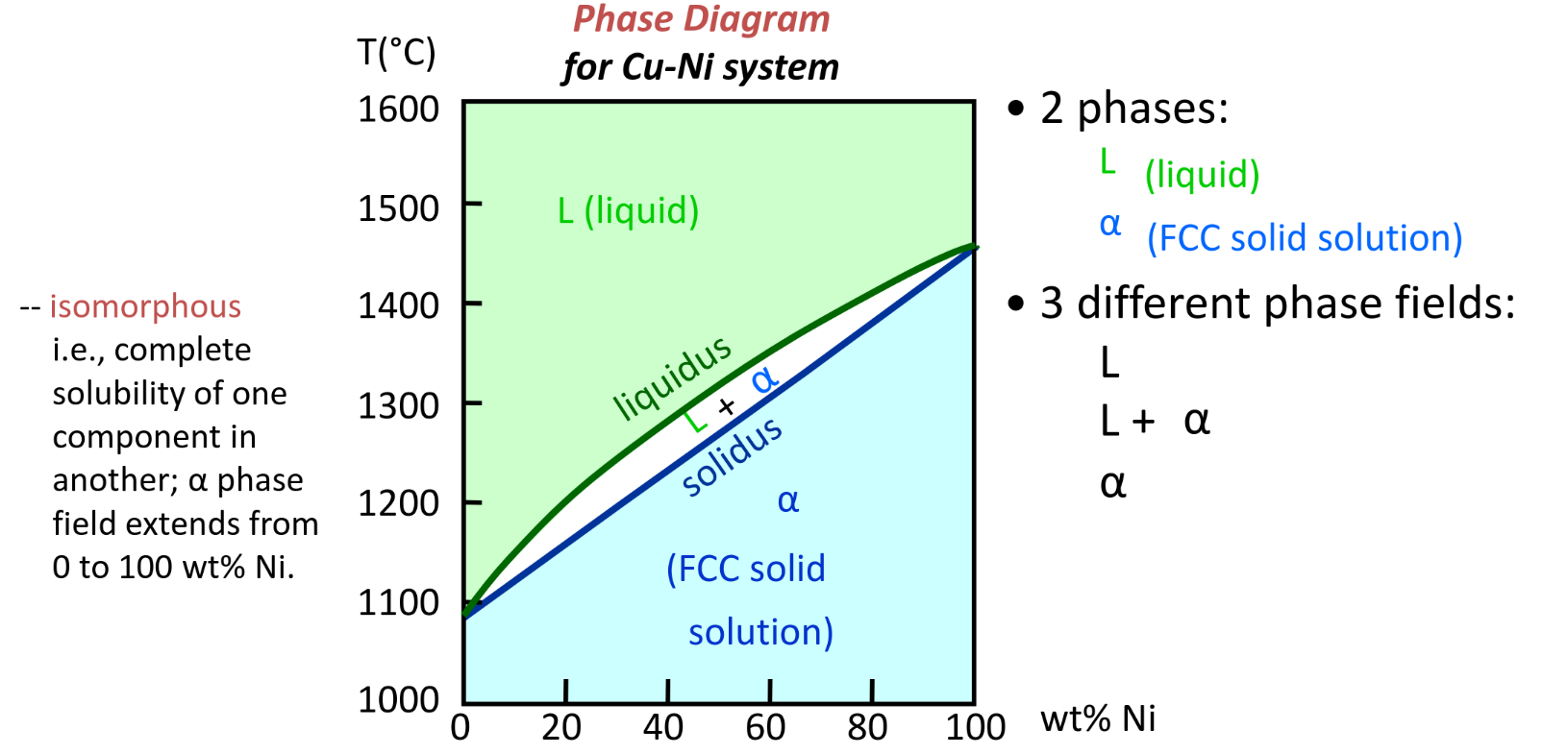
Isomorphous binary phase diagram
P = 1 atm for this course
 Weight fraction of each phase in the mixed phase can be deduced based on graphical proximity to each state
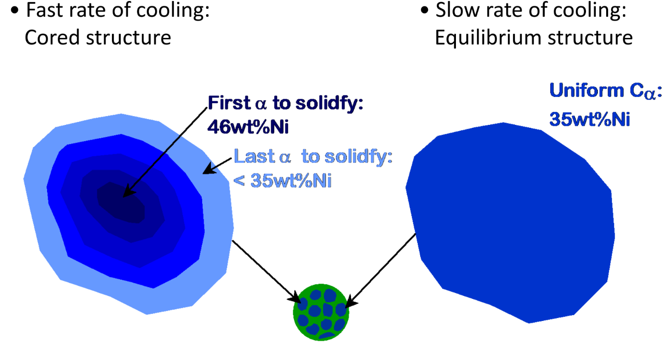
Cored vs Equilibrium phases
Weight fraction of each phase in the mixed phase can be deduced based on graphical proximity to each state
Cored vs Equilibrium phases
 Multiple phases in solid solution
Parts of the solid have different composition and crystal structure Due to: Immiscible Components — Solubility limits (Hume-Rothery rules) reached
Binary-Eutectic Systems
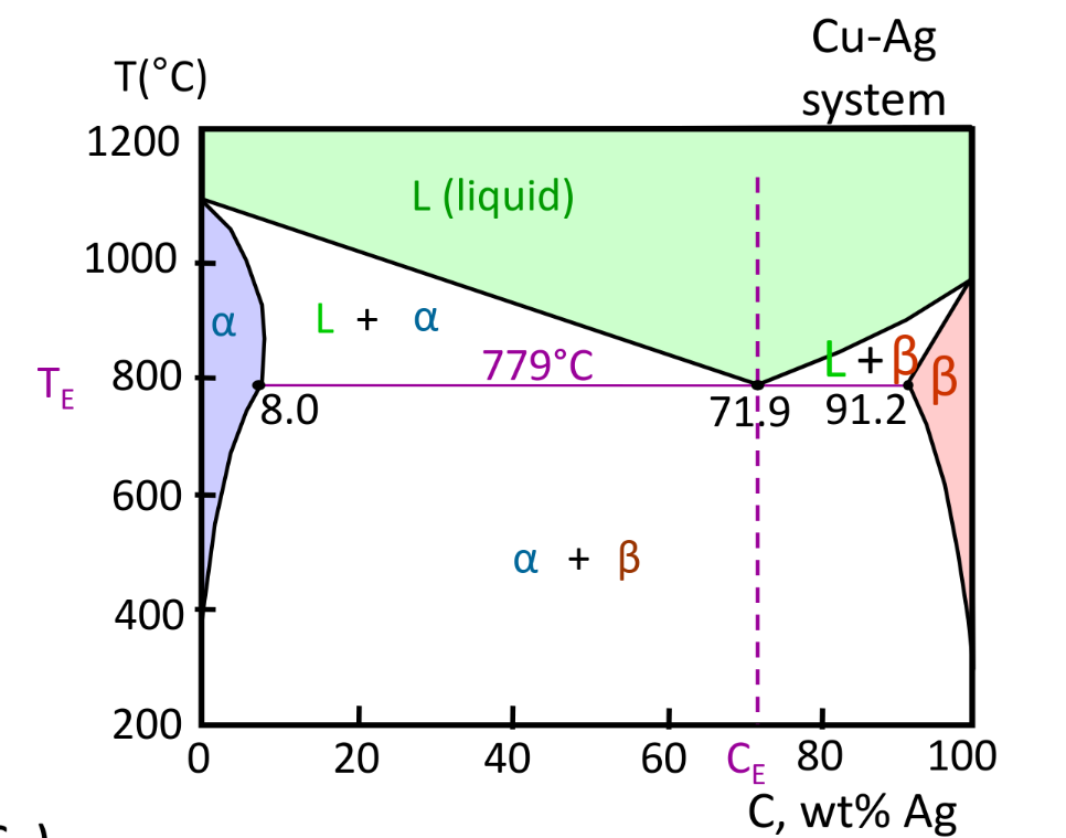
- 3 single phase regions
- Due to limited solubility
- Weight fraction is calculated the same way
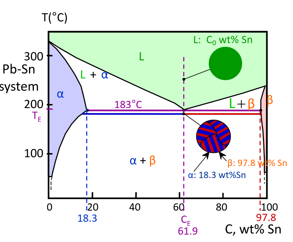
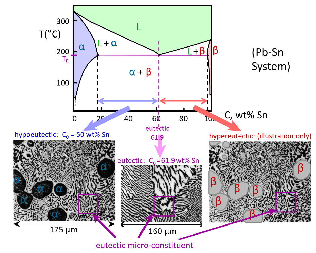
Structures in Eutectic Systems
Dual-phase Alloys
-
small beta-phase precipitates
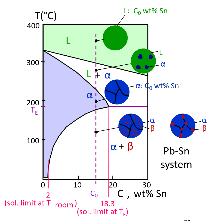
Eutectic Alloy @Ce
-
Eutectic microstructure — alternating layers of alpha and beta
Near-eutectic Alloy — Near Ce
-
particles and eutectic structure
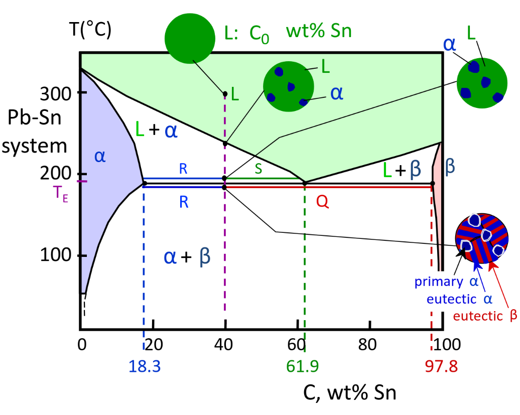
Hypoeutectic & Hypereutectic structures
Intermetallic Compounds
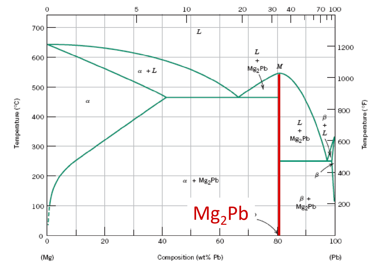
- Exists as a line on the diagram due to the fixed composition nature of ionic compounds (Stoichiometry)
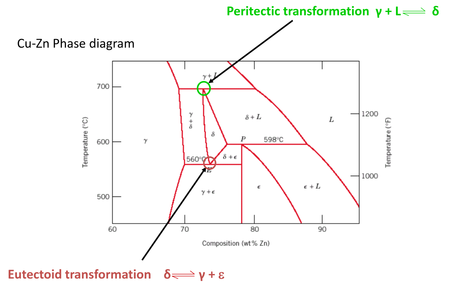
Phase transformation
Eutectic: Liquid ↔Solid1 + Solid2 Eutectoid: Solid1 ↔ solid2 + solid3 Peritectic: Liquid + solid1 ↔ solid2
-
reference
Iron-Carbon Alloys
Phase-diagram
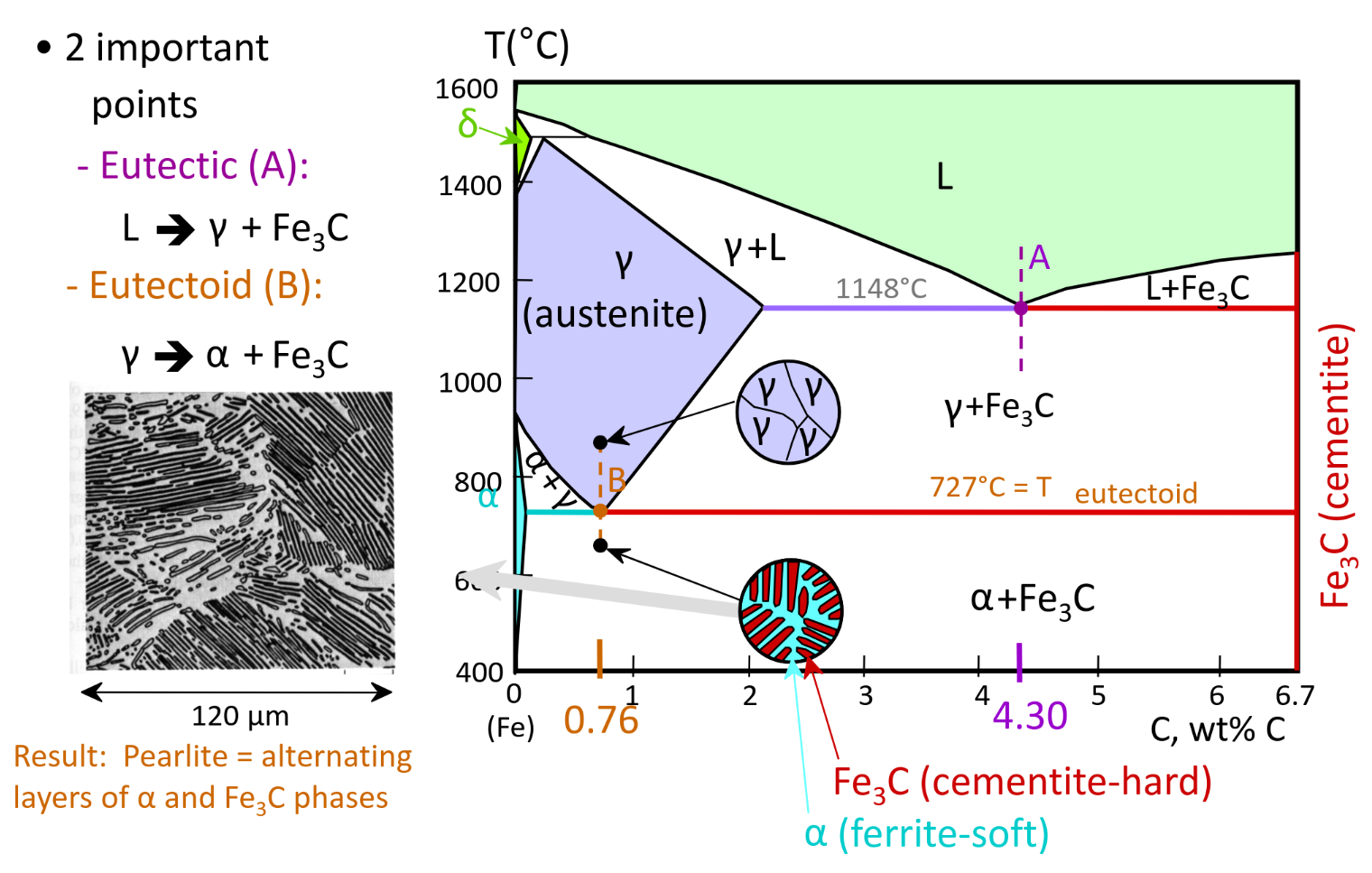 Pearlite is tough and durable — rapid quenching forms Martensite, strongest and hardest in the C-Fe system (Obtained by cooling from austenite)
Limitations: High density — Low electrical conductivity — Poor corrosion resistance
Pearlite is tough and durable — rapid quenching forms Martensite, strongest and hardest in the C-Fe system (Obtained by cooling from austenite)
Limitations: High density — Low electrical conductivity — Poor corrosion resistance
Steels < 1.4 wt% C
Hypoeutectoid Steel — Pearlite + Ferrite precipitate / streaks — < 0.76 wt%
Hypereutectoid Steel — Pearlite + Fe3C precipitate / streaks — > 0.76 wt%
 1060 steel — plain carbon steel with 0.60 wt% C
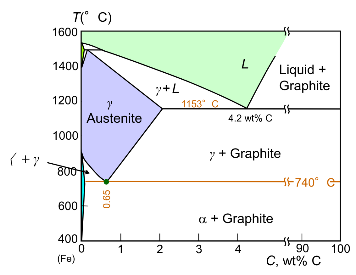
Cast Irons 3-4.5 wt% C
Brittle — Low melting — Cementite decomposes to ferrite + graphite slowly
Graphite formation is promoted by Si > 1 wt% & slow cooling (True Equilibrium Diagram)
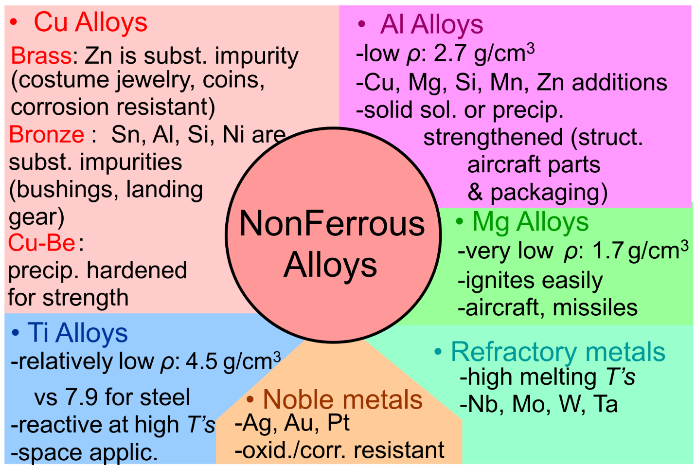
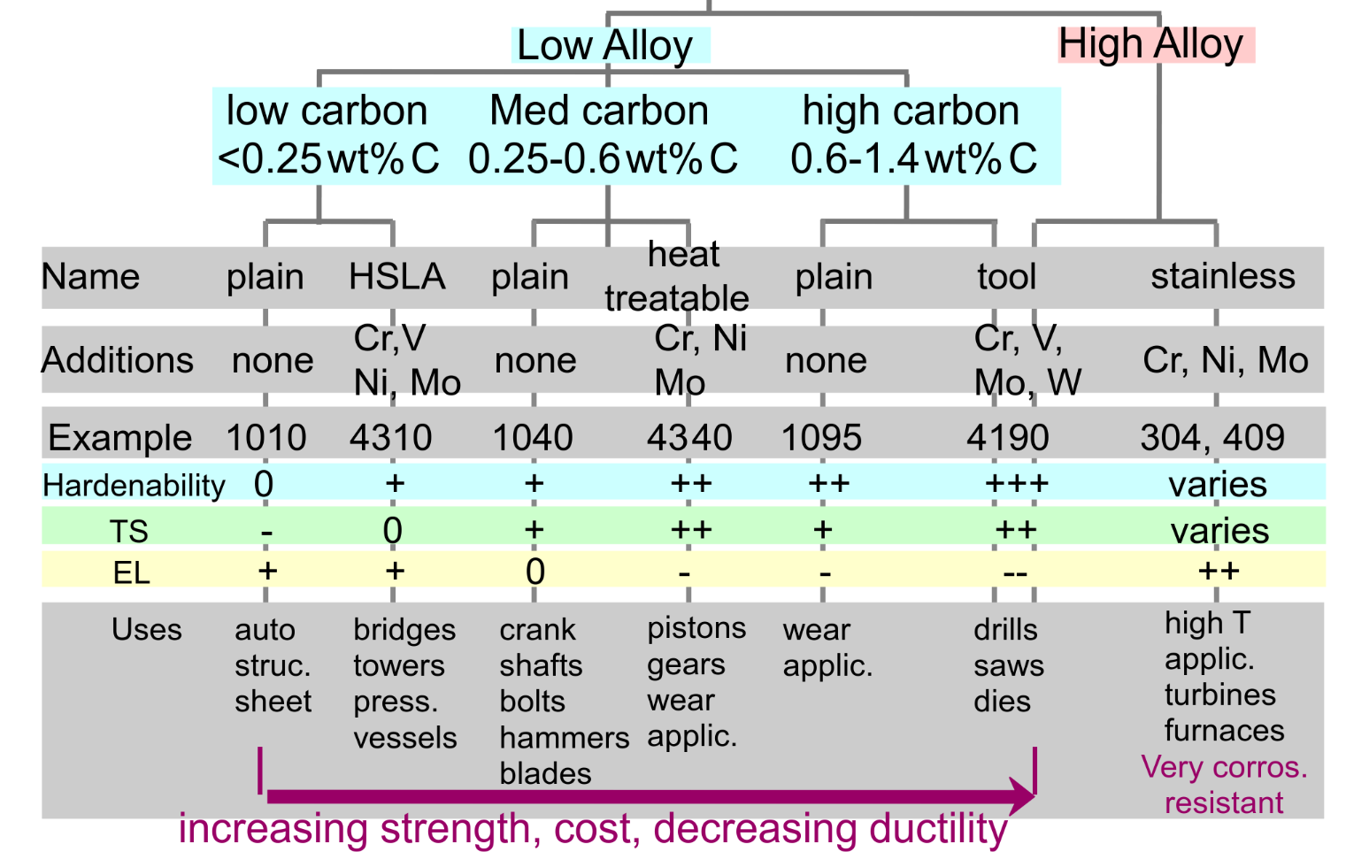
Others Non-ferrous Alloys